Device Inspection Workflow
Device Inspection Roadmap
In this guide, we will go through all the steps of setting up a Device Inspection scan for a patterned wafer, one of nSpec’s most popular and powerful workflows. Device Inspection is an nSpec analysis that detects defects by comparing scans to a generated golden template of the wafer.
First, this guide will explain how to configure all the prerequisites needed to run a patterned wafer scan. Next, these configurations will be used to run a scan followed by a Device Inspection analysis. Running the analysis for the first time will generate a golden template, which we recommend refining with subsequent scans to ensure detection is satisfactory before running a Device Inspection workflow.
The steps to setting up a Device Inspection workflow are as follows:
Create an image setting group
Use the results of step 1 to configure autofocus settings
Use steps 1-2 to create a north-south-origin alignment
Use steps 1-3 to create a focus point pattern
Use step 3 to create a device layout
Use results of steps 1-5 to setup and run a first scan with device inspection
Continue scanning to refine the golden template until detection is satisfactory
Demonstration Details
In this demonstration, we are scanning a 150 mm patterned wafer and looking for defects 0.4 μm and larger. We are placing the sample onto the center of the stage of an nSpec PS system without an autoloader, and orienting it so that the wafer flat faces west. Lastly, we are operating using access level Engineer.
Starting the Scan
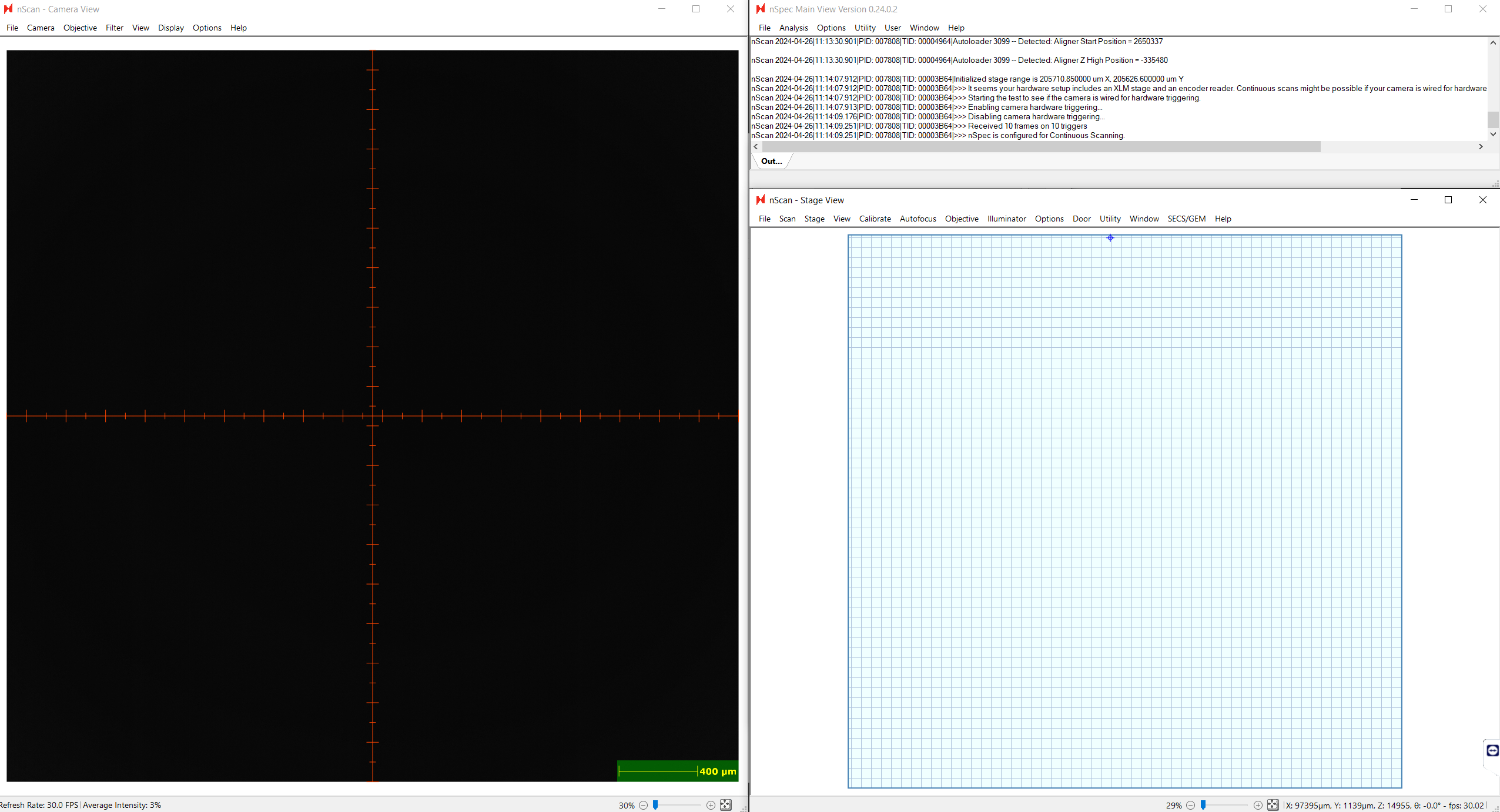
First, start nSpec. After starting up nSpec, three different windows will open – nScan - Camera View, nSpec Main View, and nScan - Stage View. In the nScan - Stage View screen, navigate to the center of grid to move the stage.
If your nSpec is setup with an autoloader, use the autoloader to place the wafer on the stage. Otherwise, to manually place the wafer on stage, first turn the chuck vacuum off by making sure nScan - Stage View > Stage > Turn On Chuck Vacuum is not enabled, place the wafer on stage, and then turn the chuck vacuum back on.
You can navigate the microscope with either the joystick, keyboard, or directly clicking the grid.
Create Image Settings Group
After loading a sample, the first step in setting up a scan is to create an image setting group. These are the lighting, resolution, and illumination modalities used to capture images during the scan.
An image setting group is a prerequisite for setting up other necessary scanning prerequisites like autofocus settings and alignment files.
Initial Steps
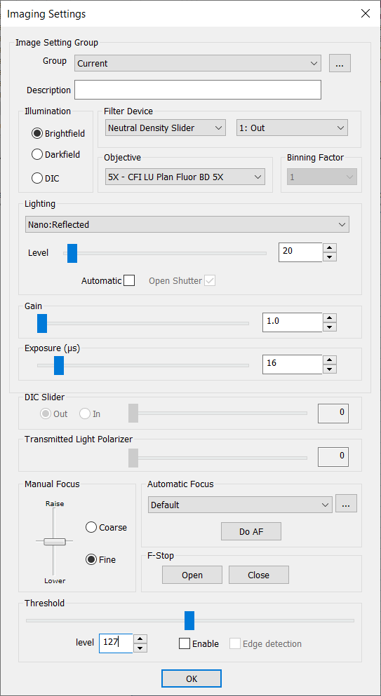
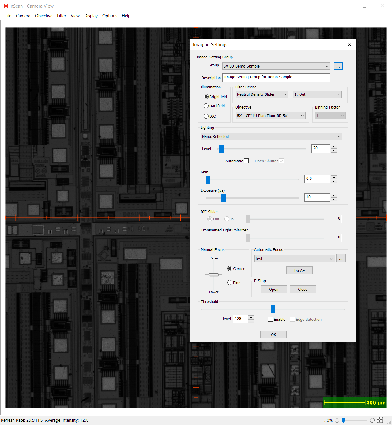
The Imaging Settings dialog can be accessed from nScan - Camera View > Camera > Imaging Settings...
First, create a new image setting group by saving the group with a name and description.

We will name this image setting group as “20x BF Demo Sample”.

Next, we recommend navigating to a region of interest on the sample – we will adjust the lighting conditions so that they are optimal for this critical region.
Use the Manual Focus section to adjust the stage height to get the sample in focus. You can also use the knob or keyboard to tune the focus. You may need to increase the lighting level as well to visualize the sample. We will fine tune the lighting conditions in the next step.
Selecting Objective, Illumination Mode, and Lighting Source
The objective, illumination mode, light source selected will depend on the properties of the sample and defects of interest. These choices will impact the scan speeds.
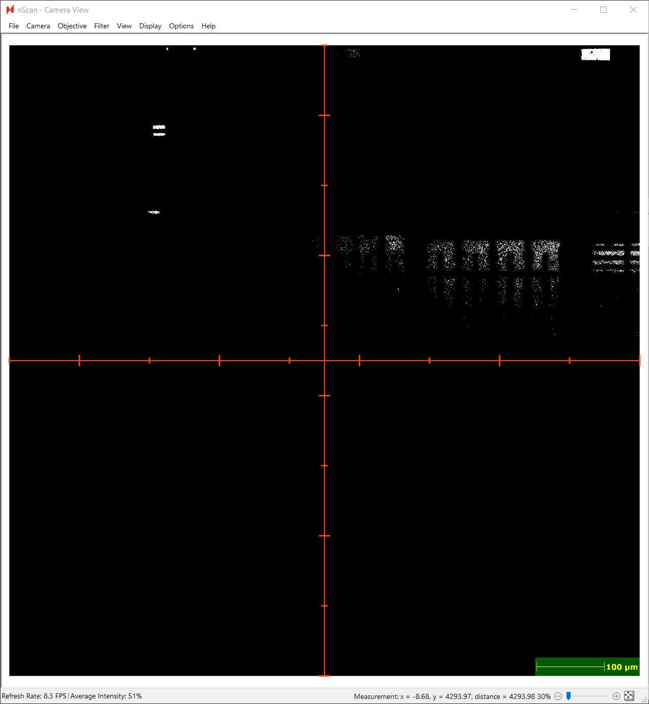
For this patterned wafer, we will choose to illuminate in Brightfield mode, which illuminates the defects of interest in a patterned wafer best. Additionally, this sample is not transparent, so we will use the Reflected lighting source instead of the Transmitted light source.
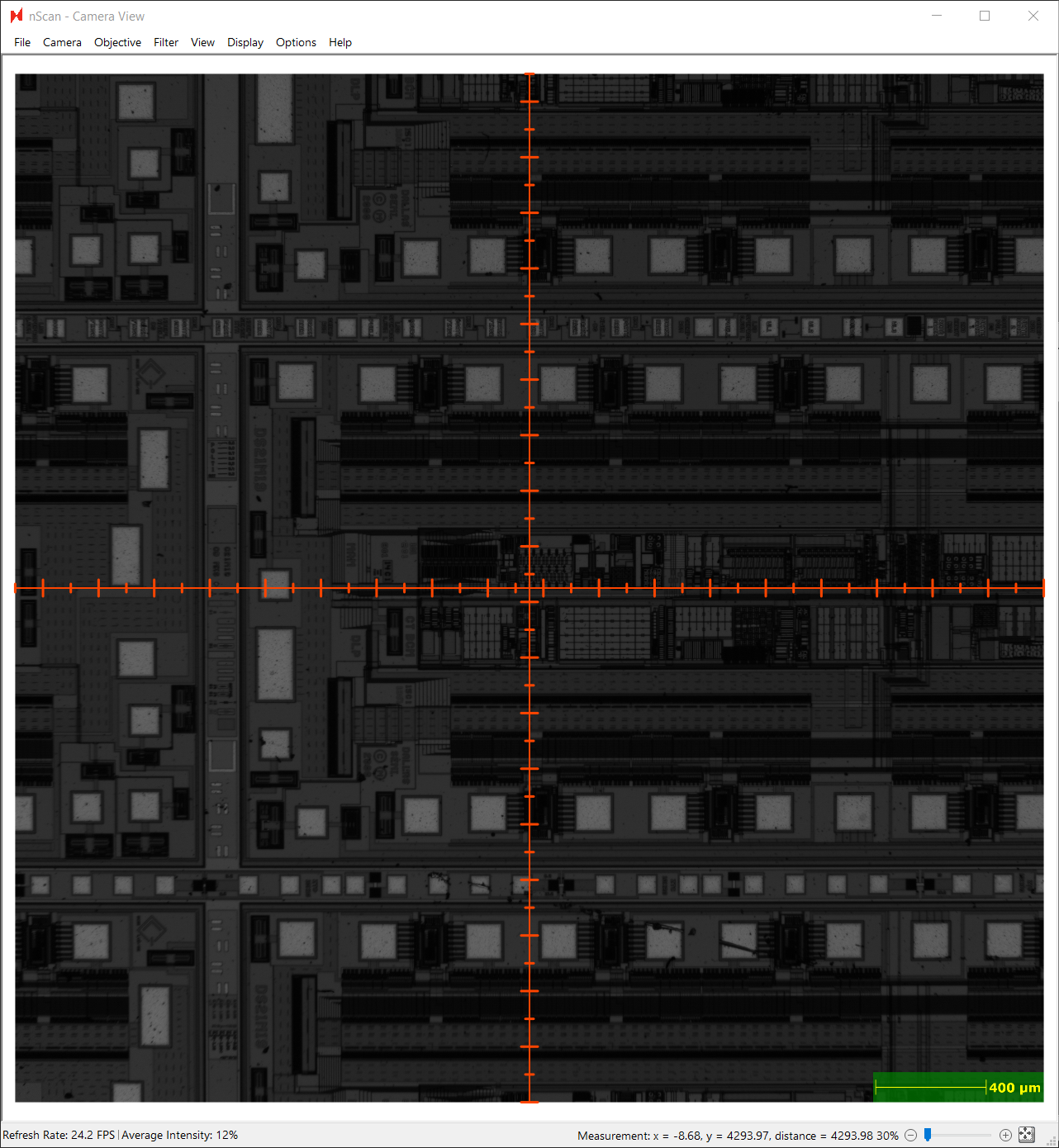
Here is the sample illuminated in Brightfield mode with Reflected lighting under a 5x objective.
We want to be able to clearly see and detect defects as small as 0.4 µm, so we will want to use a higher magnification objective. Below is a table of approximate resolution for different magnification objectives.
Objective | Resolution (μm/pixel) |
|---|---|
1.25x | 3.600 |
2.5x | 1.800 |
5x | 0.900 |
10x | 0.450 |
20x | 0.225 |
50x | 0.090 |
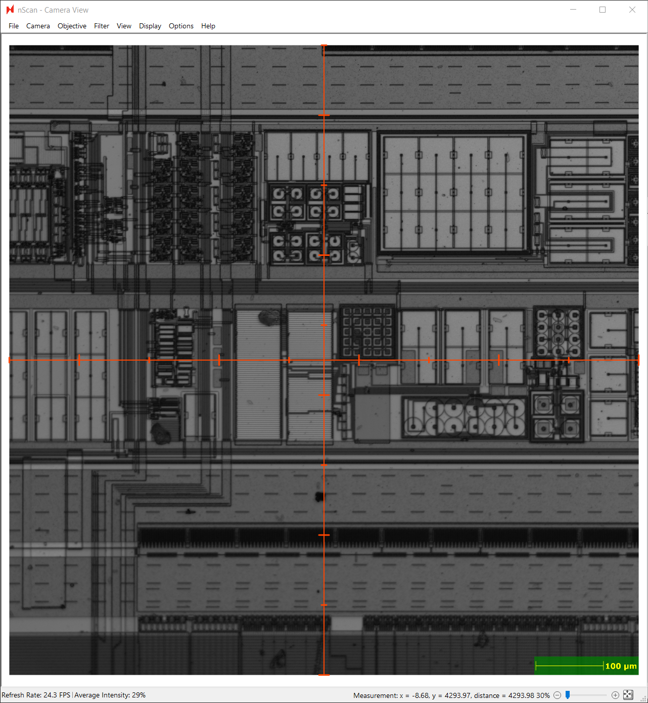
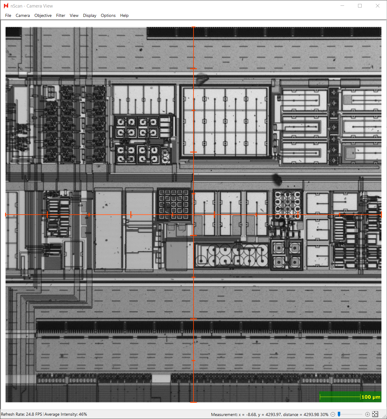
In the following image, we’ve switched to a 20x magnification objective, which provides a much clearer view of the device structures of interest. We will choose to scan with the 20x objective.
Iteratively Adjust the Lighting Conditions
There are a few different parameters that can be used to adjust the lighting conditions. The goal is to capture an image that illuminates features of interest on the patterned wafers. The image should not be oversaturated or too dark. Figuring out the optimal imaging conditions is an iterative process.
For this patterned wafer, we are most interested in looking at defects found on devices, and will optimize our lighting settings for this case.
We recommend adjusting the lighting conditions in the following order. First, adjust the Lighting Level. For this sample, we will have to raise the lighting level to 1000.
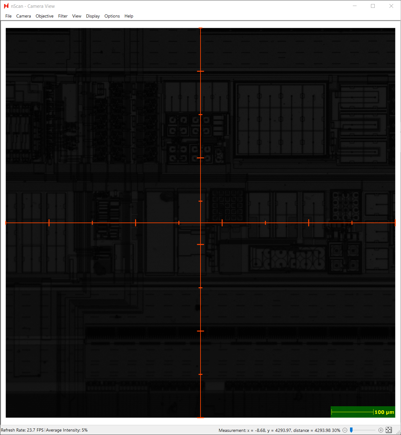
Patterned Wafer under 20x Objective, Lighting Level 1000, Gain 1.0, Exposure 10 μs
The sample is still very dark, so we will adjust the Exposure next. Increasing the exposure will allow us to image under low light conditions. This will also increase the scanning time. We will continue to increase the exposure until our features of interest can be seen clearly without being overexposed. Overexposing the sample runs the risk of decreasing the sensitivity of defect detection during Device Inspection analysis, and increases the risk of false positives.
To prevent overexposing, we recommend enabling the Threshold tool at level 240 to make sure that there are no white pixels at this level. The Threshold tool can be found at the bottom of the Imaging Settings dialog.

In the photo below, we’ve enabled image thresholding after increasing the exposure to 95 μs, while keeping lighting at 1000 and gain at 1.0. We can see that some more reflective parts of the sample in this view are still overexposed.
Decreasing the exposure to 88 μs makes these oversaturated white pixels disappear in the thresholded image view.

Below is the sample with lighting level 1000, gain 1.0 and exposure 88 μs.
Patterned Wafer under 20x Objective, Lighting Level 1000, Gain 1.0, Exposure 88 μs
We will not increase the gain for this use case because increasing the gain increases pixel intensity in software, and will result in a grainier, lower quality final image. However, sometimes it is necessary to increase the gain in order to be able to increase image brightness without increasing exposure time, which slows down scan speeds. We recommend limiting gain to 10.0 or lower to maintain image quality.
Don’t forget to save your settings.
Troubleshooting Common Lighting Issues
Image Oversaturation
If working with a highly reflective sample that is oversaturated at low lighting conditions, consider using the Neutral Density Slider under the Filter Device section, which will reduce the intensity of all wavelengths. If not addressed, oversaturation can diminish detection sensitivity and increase false positives.
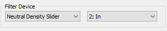
Image Flickering
If at low lighting conditions (e.g. lighting level of 100 with gain 1.0 and 10 μs exposure) and image flickering is observed, the Neutral Density Slider can be used to improve image quality. Flickering is a result of being able to observe the pulse-width modulation of LED light sources at low light, and causes light intensity variation between image tiles, resulting in weaker defect detection.
Configure Autofocus Settings
After creating an image setting group, the next step in setting up a scan is creating a set of autofocus settings. An image setting group is a prerequisite for configuring autofocus settings.
Autofocus settings are used during the scan’s autofocus step, in which the z-height of a set of focus points is calculated and used to predict the surface of the entire sample. Thus, adjusting the autofocus settings are critical to capturing consistently high-quality, in-focus images of the patterned wafer.
Accessing Autofocus Settings Dialog
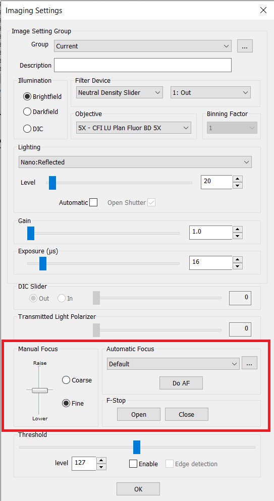
The Autofocus Settings dialog can be accessed via the three dots button in the Automatic Focus section of the Imaging Settings dialog.
Imaging Settings for Autofocus
The first thing to do is to associate the appropriate image setting group with this new autofocus setting. Double click the Group Name option, which is under Image Setting Group of the Autofocus Settings dialog, to edit the value. We will set it to “20X Bf Demo Sample”.
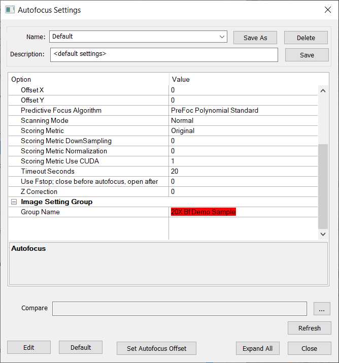
After setting the Group Name, we will save the autofocus settings as “20X BF Demo Sample”.
Note: it is not necessary to always set the autofocus setting’s image setting group to be the same as the scan’s image setting group. Depending on the use case, it be may be beneficial to choose a different illumination mode or resolution for performing autofocus.
Configuring Autofocus Parameters
Next, we’ll set some of the autofocus parameters.
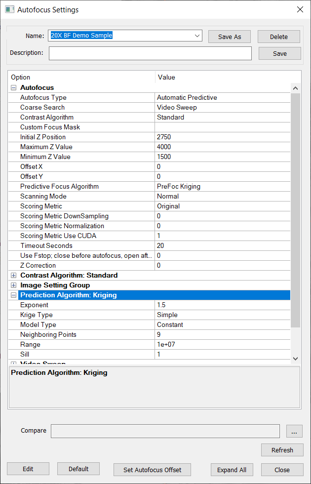
We will set the Autofocus Type to Automatic Predictive, which uses a Predictive Focus Algorithm to make predictions about the shape of the sample surface in order to automatically focus during scanning. The vast majority of use cases will use Automatic Predictive.
Then, we will set the Predictive Focus Algorithm to PreFoc Kriging. This is a good option when performing 20x and higher magnification scans, and when performing scans with irregular focus point patterns. When performing scans of smaller magnifications like 10x or lower, Prefoc Polynomial Standard works well with regular focus point patterns like circles and squares. We recommend running Prefoc Polynomial Standard with default parameters. For more information about choosing an autofocus algorithm, read the Surface Predictors guide Predictive Focus Algorithms.
Next, we will set Use FStop to 0 to disable F-stop use. F-stop use is necessary to find focus for bare wafers, but is unnecessary for most patterned wafers.
You must save the settings again in order for additional option-specific parameter groups to appear in the Autofocus Settings dialog. For example, the Prediction Algorithm: Kriging group does not appear by default – you must select PreFoc Kriging as the Predictive Focus Algorithm and then save the settings.
After saving the above parameters, we will expand the Prediction Algorithm: Kriging group and set the Model Type to Constant.
The last step is to click the Set Autofocus Offset button at the bottom of the autofocus dialog, which will set the Initial Z Position value to the current Z position of the sample. This should be done while the sample is in focus.
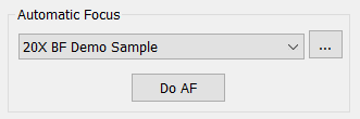
Save the autofocus settings, close the dialog, set Automatic Focus in the Imaging Settings dialog to “20X BF Demo Sample”, then click Do AF.
Create North-South-Origin Alignment
North-South-Origin alignment uses a north, south, and origin point to align the camera to a patterned sample during scanning. Setting up an image setting group and autofocus are prerequisites to setting up alignment.
Navigate to the Device Inspection Alignment wizard via nScan - Full Stage View > Scan > Device Inspection Alignment > Start Wizard…
Choosing Alignment Points
In this dialog, you will select three points on the wafer to align the camera and layout file to the sample’s pattern – a north point, south point, and origin point. nSpec uses a cross-correlation based algorithm to match the chosen alignment points to the sample.
The north and south points chosen are ideally unique structures on the wafer that are directly north and south of each other. If there are no unique structures on the wafer, the structure chosen needs to be unique within a single field of view.
This sample has been loaded manually with the flat oriented towards west. The flat can be oriented towards any cardinal direction: north, east, south, or west.
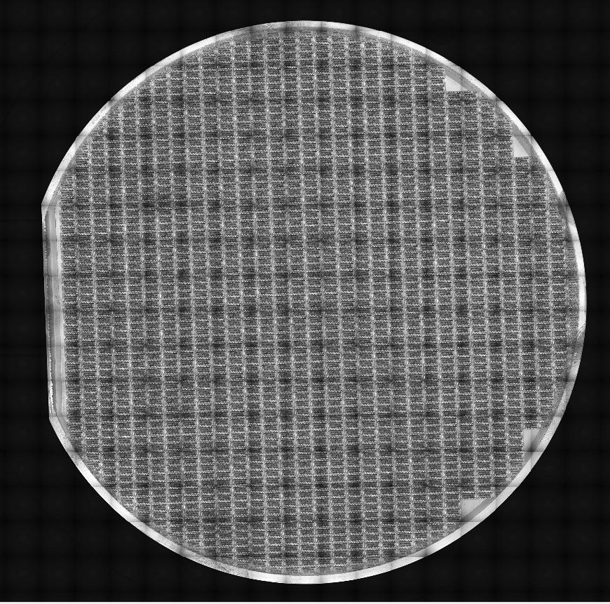
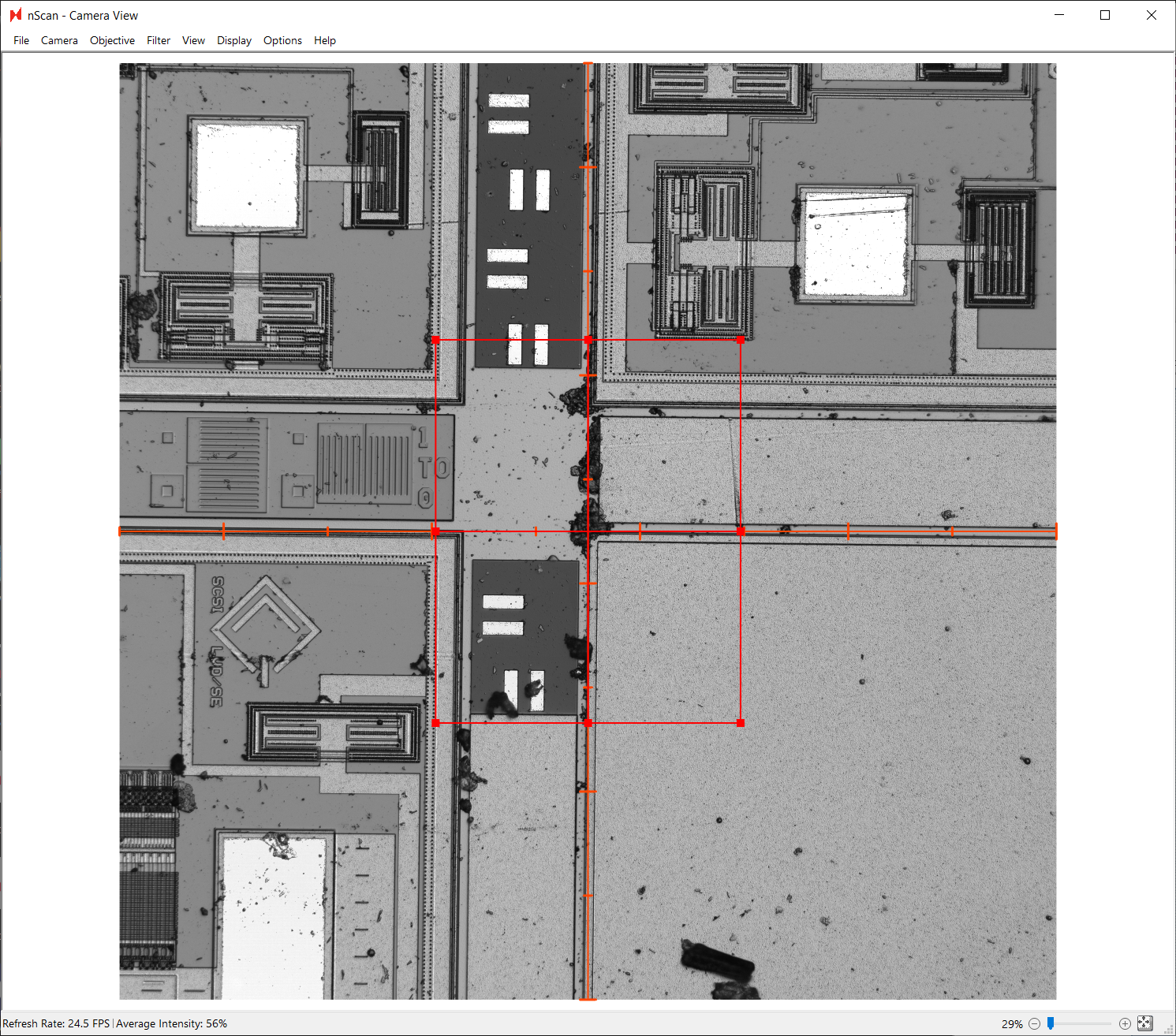
Looking at a 2x scan of the wafer below, we can see that there are no unique fiducial markings on this wafer. However, there are unique structures that we can choose as our north and south alignment points.
There are two pairs of unique features on the wafer that could be potentially be used for our north and south alignment points. Either set of north-south pairs could be used, however, north point option 1 and south point option 1 are a more optimal pair than north point option 2 and south point option 2, because there is more distance between the option 1 pair than the option 2 pair.
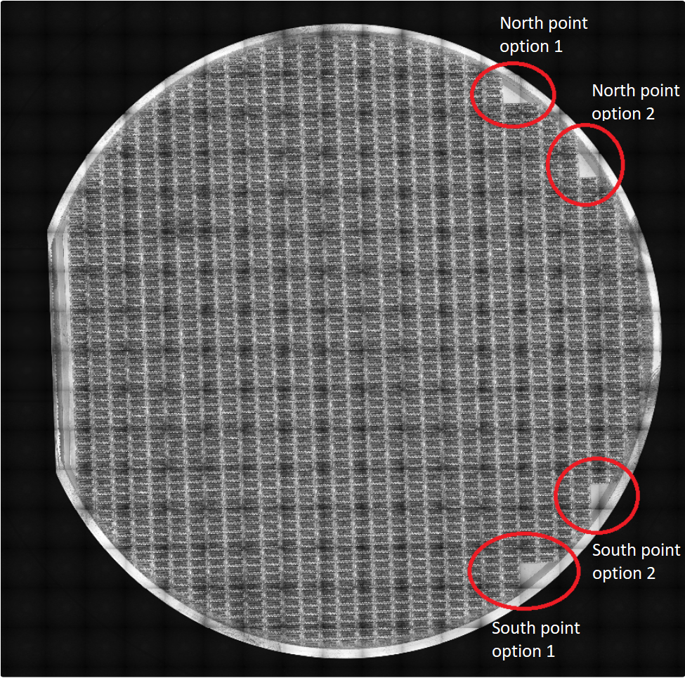
Looking closer at north point option 1, we will choose the corner of the bare portion as the center of our alignment point.
Define North
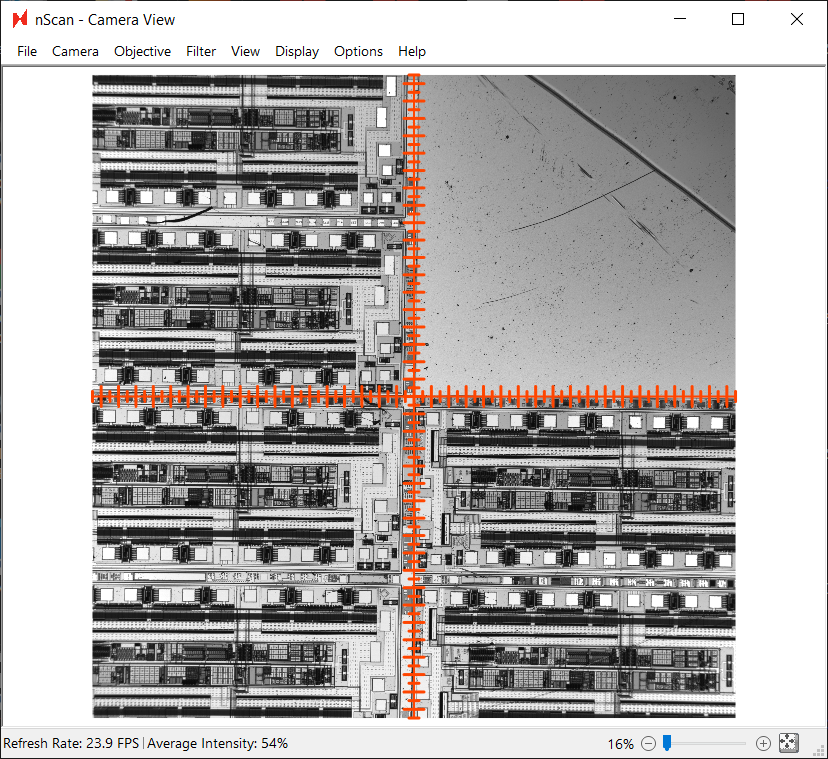
Once the alignment dialog is open, point to your autofocus settings and image setting group. Before continuing on and clicking Next, you must define “North” on your wafer, which is defined by drawing a bounding box in the nScan - Camera View window.
For best results, we performed the following steps to draw the bounding box.
Click the expand to fit button in the bottom right corner of the Camera View.
Click and drag a bounding box centered on the corner of the blank area as the center. We recommend that bounding boxes should be roughly 1/4 the size of the field of view.
Zoom in to make sure that the bounding box is truly centered. Correct if necessary.
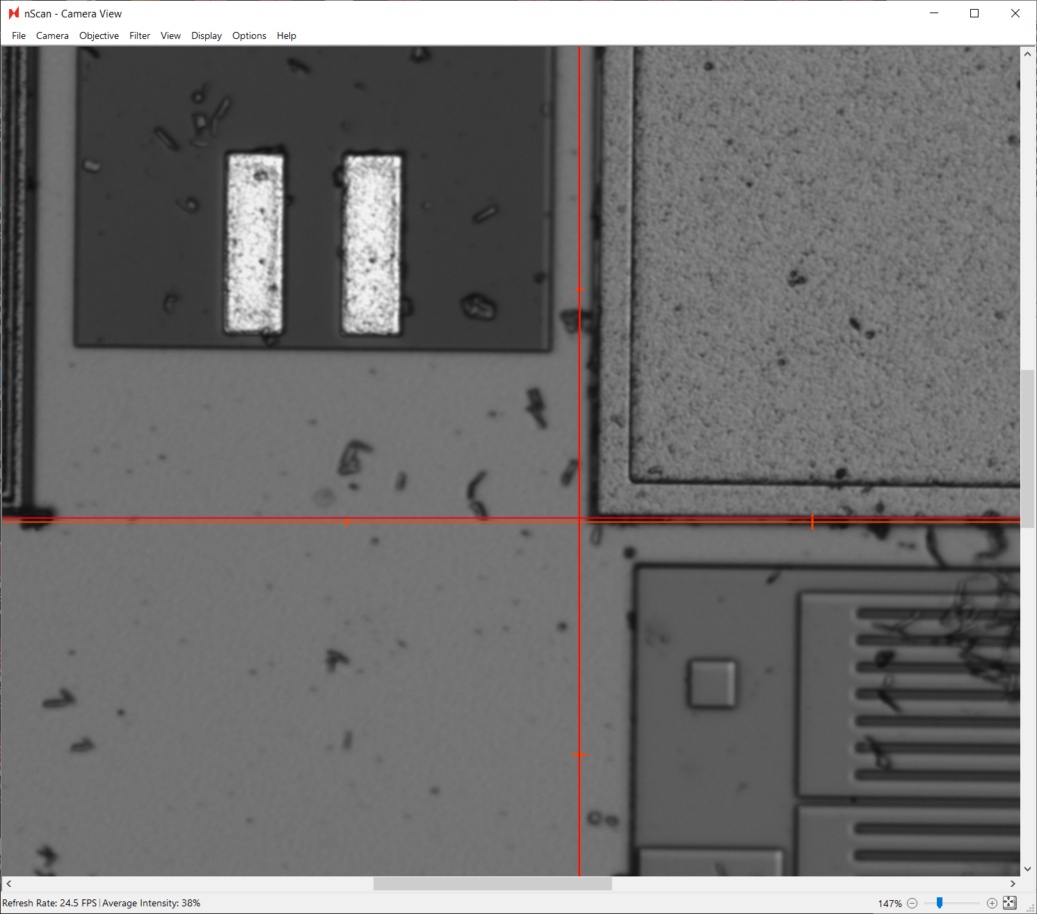
The center of the bounding box was not perfected aligned to the corner in the screenshot above, and has been corrected in the screenshot below.
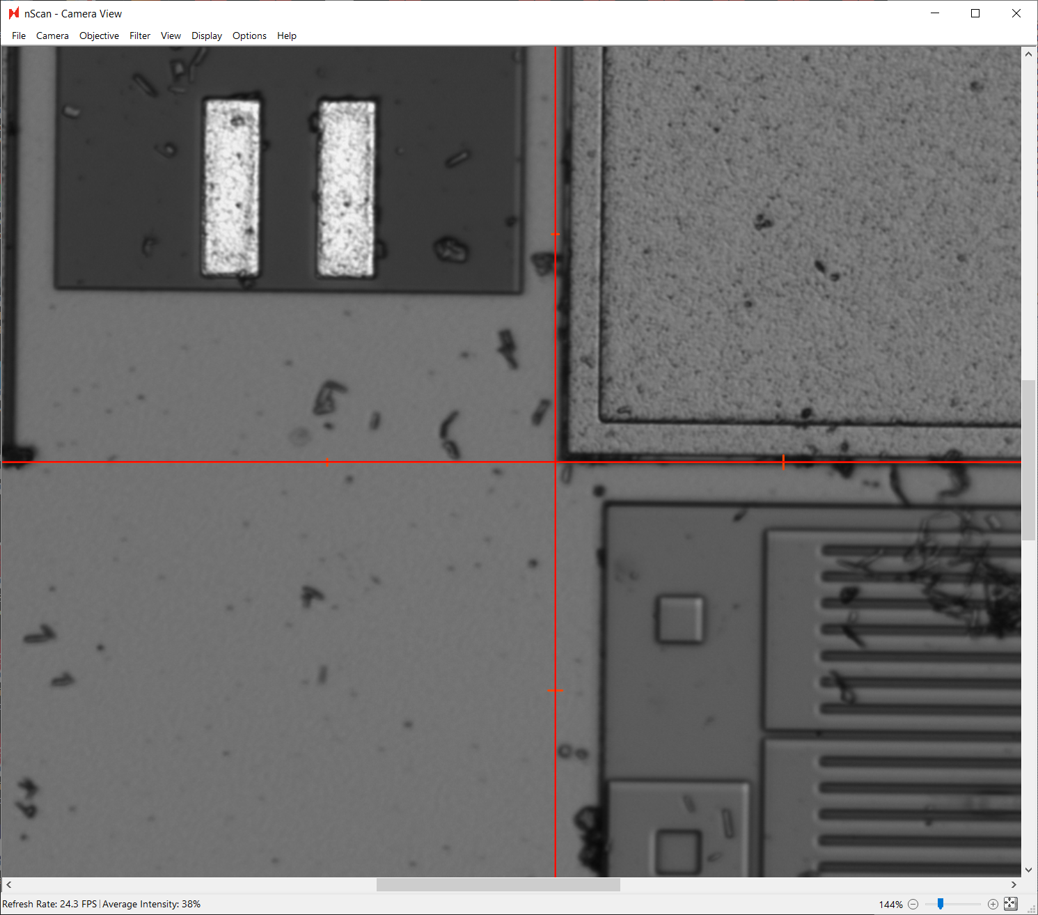
Now that the north alignment point is defined, click Next.
Define South
Next, we will define the south point. Again, we will set the autofocus and image setting group to the settings created before.
We highly recommend using the bounding box drawn to define the north alignment point to capture the south alignment point. Additionally, we recommend using the joystick or down arrow key to navigate towards the south point.
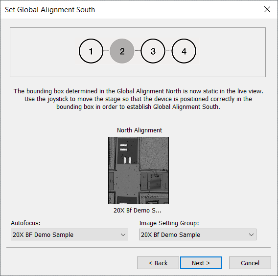
Here, we are choosing the corresponding unique structure, directly south of the chosen north alignment point. Click Next.
Define Origin
Lastly, we will define the origin, which defines the (0,0) coordinate of the wafer.
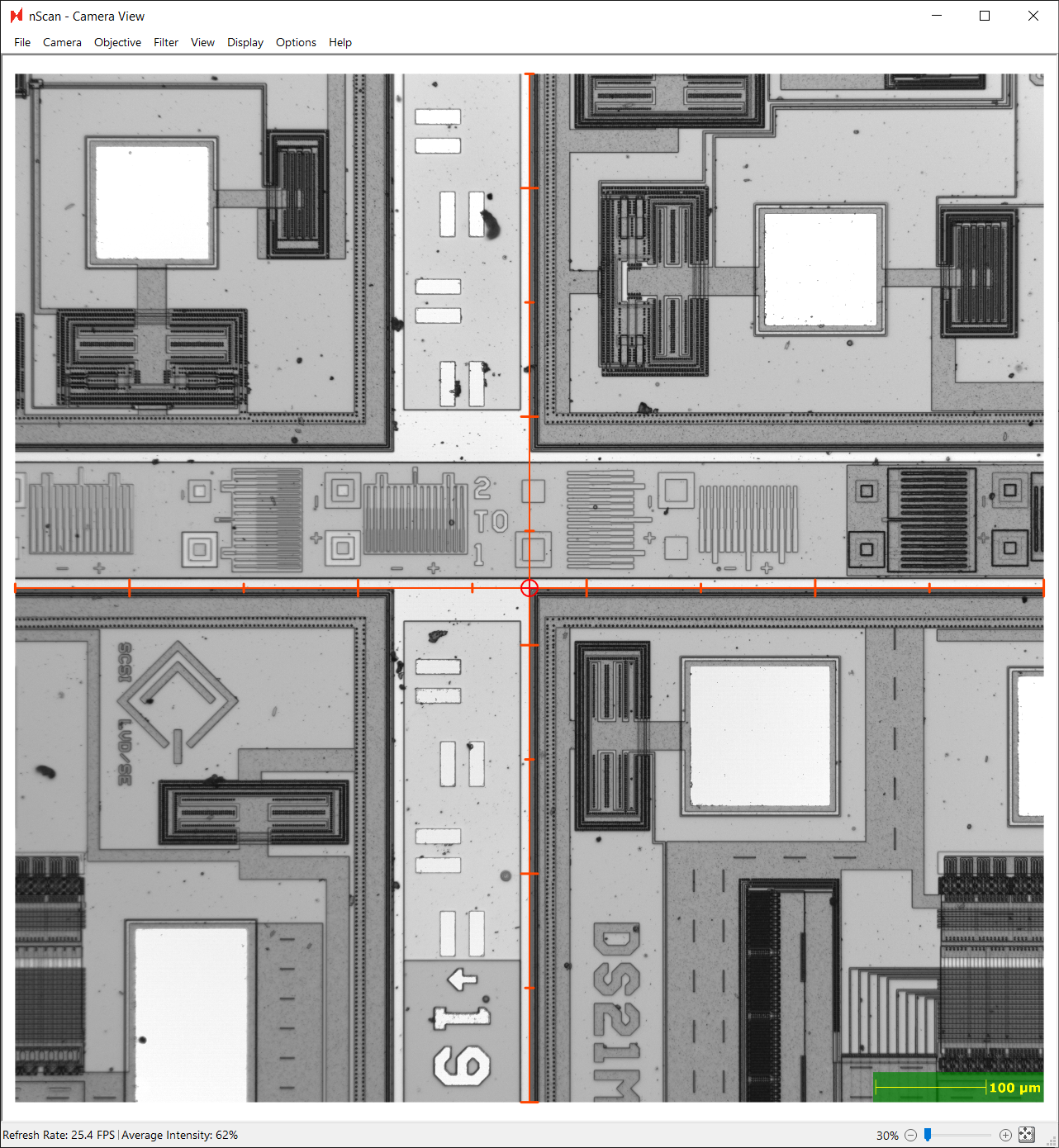
Any point can be defined as the origin, and we will choose a point close to the wafer center as our origin point. The center of the stage is roughly 102,000 by 102,000 µm. Because this sample was carefully placed in the center of the stage, we can assume the wafer center is near the stage’s 102,000 µm, 102,000 µm point. We will temporarily switch to a lower magnification objective to aid in finding the center point.
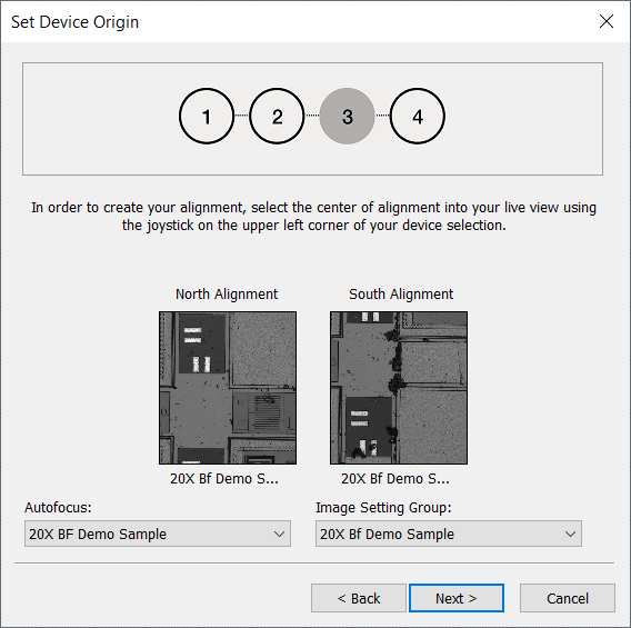
Once we’ve arrived at the central intersection of this patterned wafer, we will select the top-left corner of the device closest to the wafer center as the origin point. Again, we will set the autofocus and image setting group settings. Click Next.
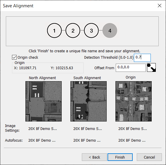
Finishing Alignment
The final step in creating the alignment file is to set the Detection Threshold to 0.7. A higher threshold fine--tunes the fiducial detection algorithm to be more conservative.
Click Finish. A dialog to save the alignment as a CSV file will appear. We will name ours “Demo Wafer Alignment.csv”.
Create Focus Point Pattern
After creating an alignment, users must create a focus point pattern as a prerequisite to scanning a sample. Creating an image setting group and autofocus setting are prerequisites to creating an alignment file, which is a prerequisite to creating a focus point pattern.
The focus point pattern indicates where the system will measure the sample’s z-heights. These z-height measurements are used as inputs to a surface prediction algorithm, which is used to predict what the focus should be set to across the sample during scanning.
The focus point pattern dialog can be found at nScan - Full Stage View > Scan > Edit Predictive Focus Patterns…
To start, name and save the pattern as “Demo Wafer Focus Point Pattern”. Next, load the alignment file created in the previous step.
After loading the alignment file, we will set the origin as a focus point. To do this, we will navigate to the origin with the Move to Origin button. Once at the origin, click the Add Point button at the bottom of the dialog, which will add the origin point to the list of focus points.
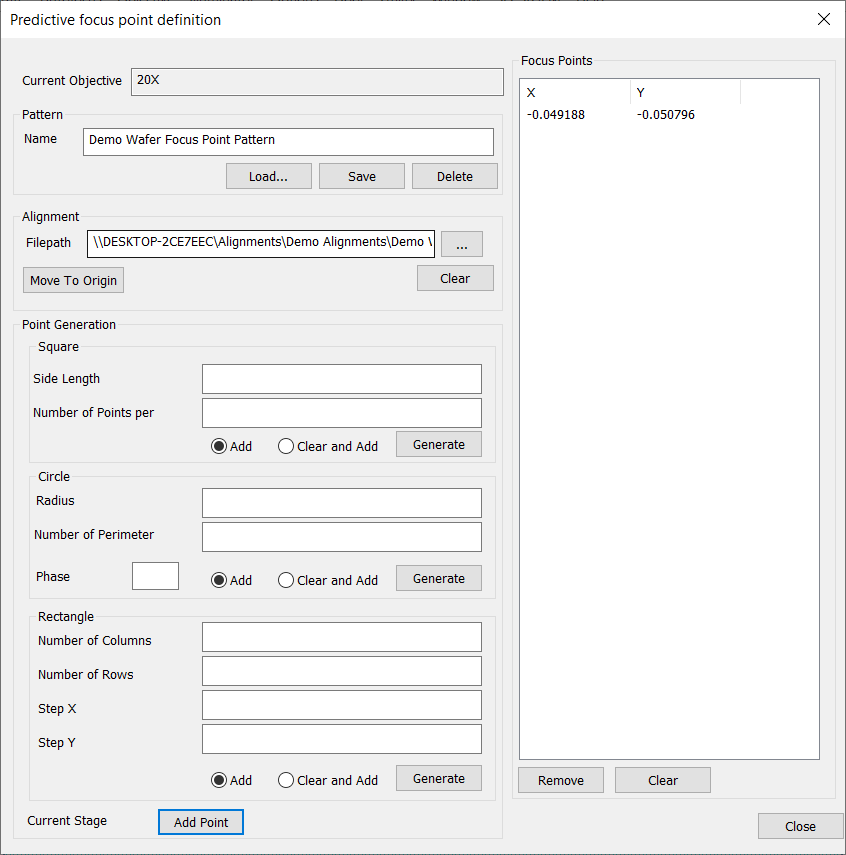
Creating the focus point pattern is straightforward. We recommend using a 16 point Kriging circle, which is a pair of concentric circles. We recommend choosing the outer ring of points to be 5-10 mm from edge of the wafer, and then inner ring to be about half way between the outer ring and center.
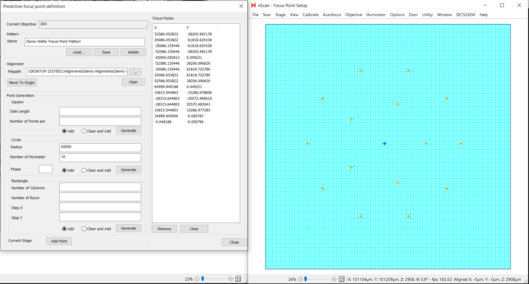
For this 150 mm diameter sample, we will set the outer ring of 10 focus points, 65 mm from the wafer center, and set the inner ring of 5 focus points, 35 mm from the wafer center.
The Radius field is in µm. To generate the first set of points, we will set Radius as 35000 and Number Of Perimeter as 5, select the Add radio button, then click Generate.
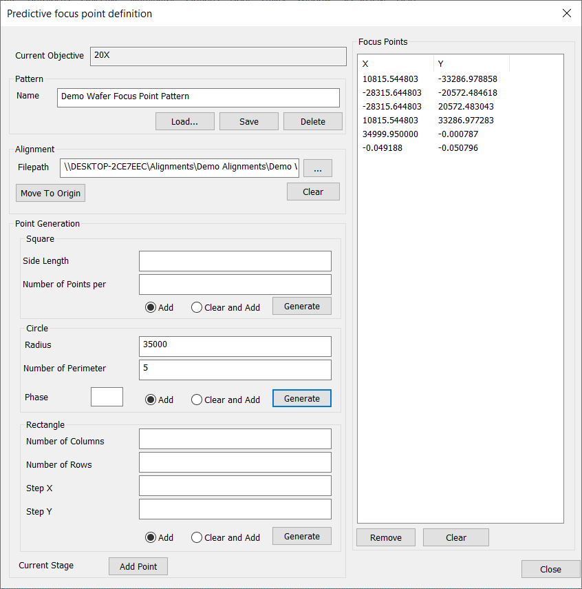
To generate the second set of points, we will set Radius as 65000 and Number Of Perimeter as 10, select the Add radio button, then click Generate. The generated focus points will appear on the stage view.
Click each point in the nScan - Focus Point Setup window to verify that each point is on the wafer.
To finish, click Save, then Close.
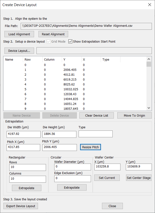
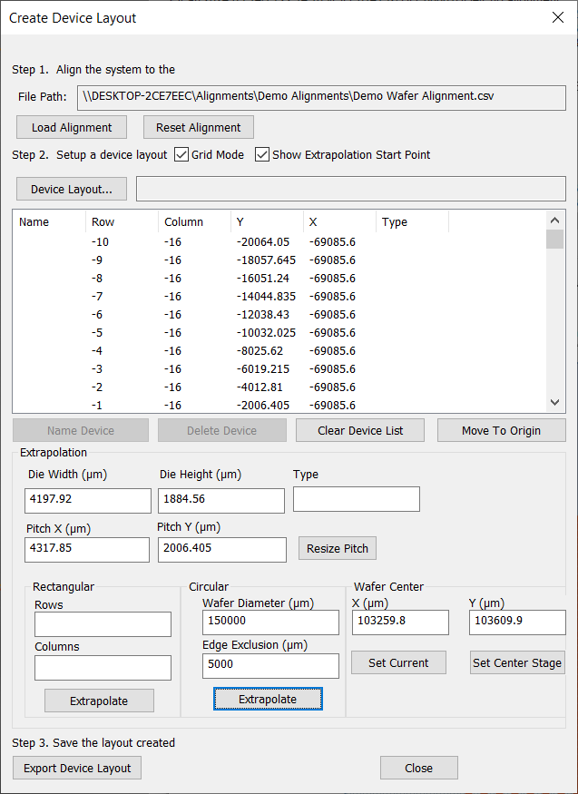
Create Device Layout
Creating a device layout is an important step in preparing to scan a patterned sample, as the layout file contains information about a patterned sample’s device sizes and coordinate locations, as well as the die pitch. Configuring an image setting group, autofocus setting, and north-south-alignment are necessary prerequisites to creating a device layout.
There are three methods for creating a device layout.
Import the device layout from a GDSII file. Note that the origin defined in the GDSII file should be the same as the origin defined in the north-south-origin alignment file.
Translate known device coordinates into an nSpec layout format.
Use nSpec’s device layout creation tool to manually create a layout.
Importing Device Layout from GDSII File
The simplest way to create a device layout file is to simply use an existing GDSII File. Step by step instructions can be found at GDS Layout Creation.
First, open the device layout creation dialog via nScan - Stage View > Scan > Create Device Layout…
Next, load the alignment created during device inspection alignment (aka north-south-origin alignment). The origin defined in the alignment file must match the origin of the GDS file.
After alignment is performed, click the Device Layout… button, then click GDS to import the file. Next, select the appropriate layer to import.
If the import is successful, the device table below will populate with device positions. Click Export Device Layout to finish layout creation.
Creating nSpec Layout from Device Coordinates
Given a set of device coordinates and die pitch values, the nSpec device layout can also be created by formatting the data into a CSV file.
Below is an excerpt of the nSpec device layout CSV file for this wafer. Starting at line 7, each line represents a device’s x and y coordinates, their device coordinates relative to the origin defined during north-south-alignment, the device width and height, name (optional), and type (optional).
Version 1
DiePitchX 4318.168000
DiePitchY 2006.610000
KlarfMode 1
BeginDelimitedListing
Id,X,Y,Xindex,Yindex,W,H,Name,Type
1,-64772.5,-30099.1,-15,-15,4197.92,1884.56,,
2,-64772.5,-28092.5,-15,-14,4197.92,1884.56,,
3,-64772.5,-26085.9,-15,-13,4197.92,1884.56,,
4,-64772.5,-24079.3,-15,-12,4197.92,1884.56,,
5,-64772.5,-22072.7,-15,-11,4197.92,1884.56,,
6,-64772.5,-20066.1,-15,-10,4197.92,1884.56,,
7,-64772.5,-18059.5,-15,-9,4197.92,1884.56,,
8,-64772.5,-16052.9,-15,-8,4197.92,1884.56,,
9,-64772.5,-14046.3,-15,-7,4197.92,1884.56,,
10,-64772.5,-12039.7,-15,-6,4197.92,1884.56,,
11,-64772.5,-10033,-15,-5,4197.92,1884.56,,
12,-64772.5,-8026.44,-15,-4,4197.92,1884.56,,
13,-64772.5,-6019.83,-15,-3,4197.92,1884.56,,
14,-64772.5,-4013.22,-15,-2,4197.92,1884.56,,
15,-64772.5,-2006.61,-15,-1,4197.92,1884.56,,
16,-64772.5,0,-15,0,4197.92,1884.56,,
Manually Create Device Layout
Obtaining the Wafer Center with Bare Wafer Alignment
Before creating the device layout, we will use Bare Wafer Alignment in order to find the location of the wafer center, which is used when extrapolating devices for circular samples.
Create Image Setting Group
Bare wafer alignment is best performed with lower magnification objectives, so we will quickly setup an image setting group named “5x- Demo Bare Wafer Alignment Settings” using the 5x objective. The automatic focus settings will not be used in bare wafer alignment, so it’s not necessary to adjust them.

Running Bare Wafer Alignment
Next, we will run bare wafer alignment. Navigate to the dialog via nScan - Full Stage View > Bare Wafer Alignment > Start Wizard…
Most default settings run well, but we will decrease the Pixels in Line parameter from the default of 150 to 80.
This parameter depends on the size and shape of the fiducial, as it determines the number of pixels used to find the wafer fiducial. If the value is too high, it may not detect the fiducial. If it is too low, it may falsely detect other structures on the wafer edge as the fiducial.
Next, we will set Wafer Fiducial to Single Flat and set Image Settings to the “5x- Demo Bare Wafer Alignment Settings”.
Under Wafer Trace Settings, we will increase the Edge Trace Speed to 20,000 µm/s to increase the speed of the bare wafer alignment process. We will also note the location of the wafer fiducial by clicking the “W”.
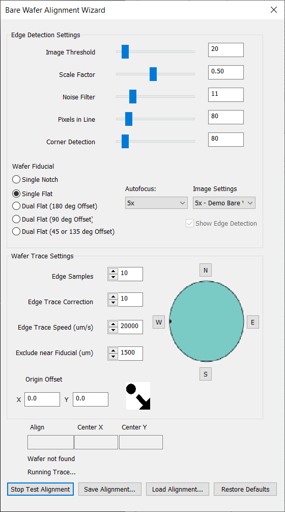
After setting all of these parameters, we will Test Alignment. After the alignment is performed, the Center X and Center Y fields will populate with the wafer center values found during alignment.
For this wafer, the center is at (103,259.8, 103609.9). Write these values down for the following device layout creation step. Additionally, you will see all the found points in nScan - Full Stage View.
Make sure to click Save Alignment…

Starting Device Layout Creation
After finishing bare wafer alignment, open the device layout creation dialog via nScan - Stage View > Scan > Create Device Layout…
First, load the alignment created during device inspection alignment (aka north-south-origin alignment). The system will perform alignment.
Next, input the wafer center values found during bare wafer alignment. Set Current will automatically input the current stage position as the wafer center values.
We will keep the Grid Mode box checked, because the patterned wafer we are scanning has uniform pitch X and Y values throughout the wafer.
Measuring Device Size
Next, we will use the Long Distance Measurement Tool found at nScan - Camera View > View > Long-Distance Measurement to measure the device size. Selecting the measurement tool changes the cursor in nScan - Camera View to a red target.
To measure the device size, click the top left corner of any device, then without clicking the screen, navigate to the bottom right corner of the same device and click the bottom right corner. We recommend using the zoom feature to be able to choose the measurement locations as precisely as possible.
Once clicking these two points, a measurement will appear in the bottom right corner of the nScan - Camera View screen. In this example, x = 4197.92, y = 1884.56. The measurement values are in µm.

Measuring Pitch Size
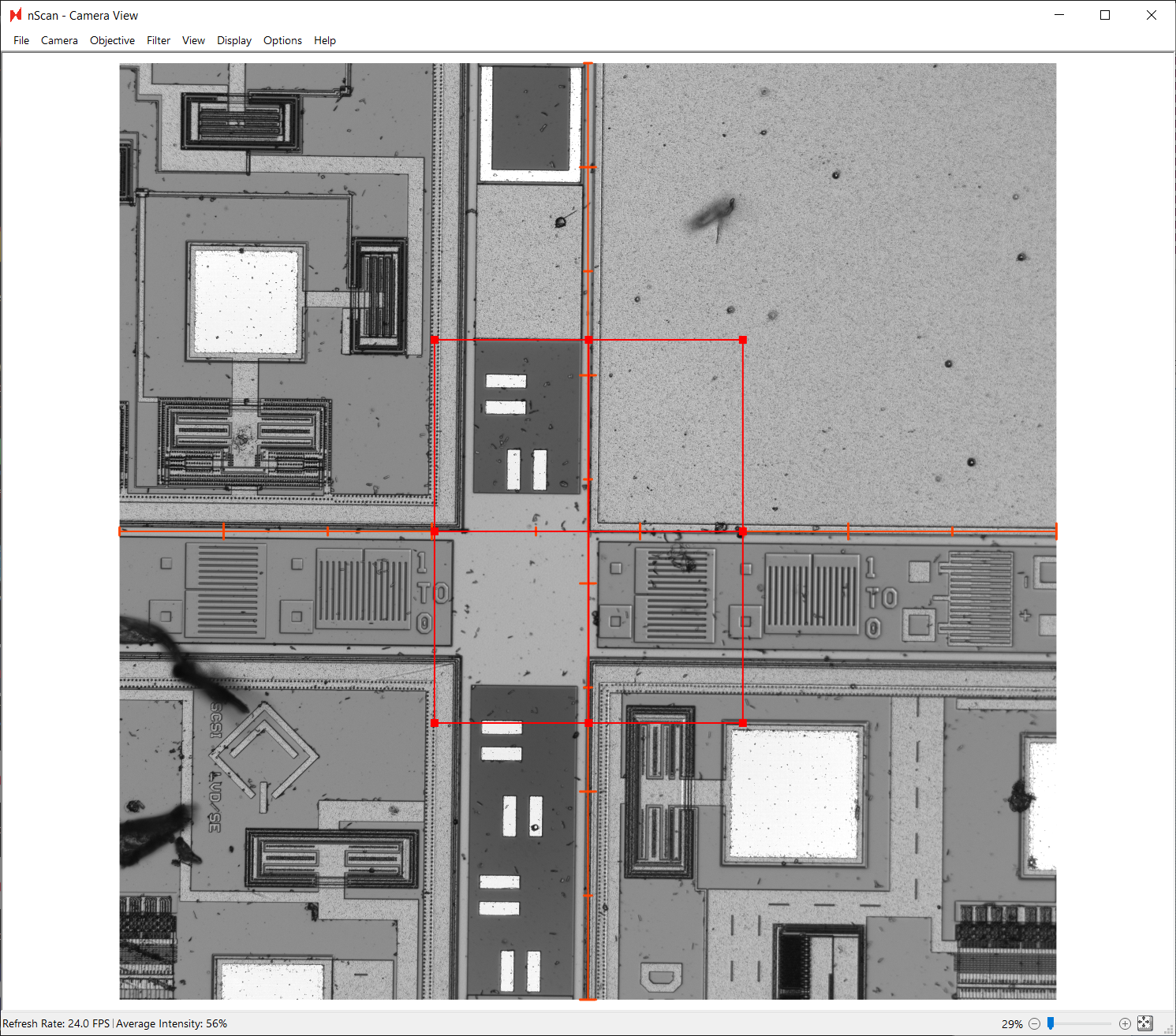
Next, we will measure the pitch size. Pitch for a given axis is the distance between the same point on adjacent devices. We will use the Long-Distance Measurement tool again to measure the pitch X and pitch Y.
The quickest way to measure both pitch X and Y is to measure between the same point on two devices that are directly diagonal to one another. In the diagram below, these measurement points are marked with stars.
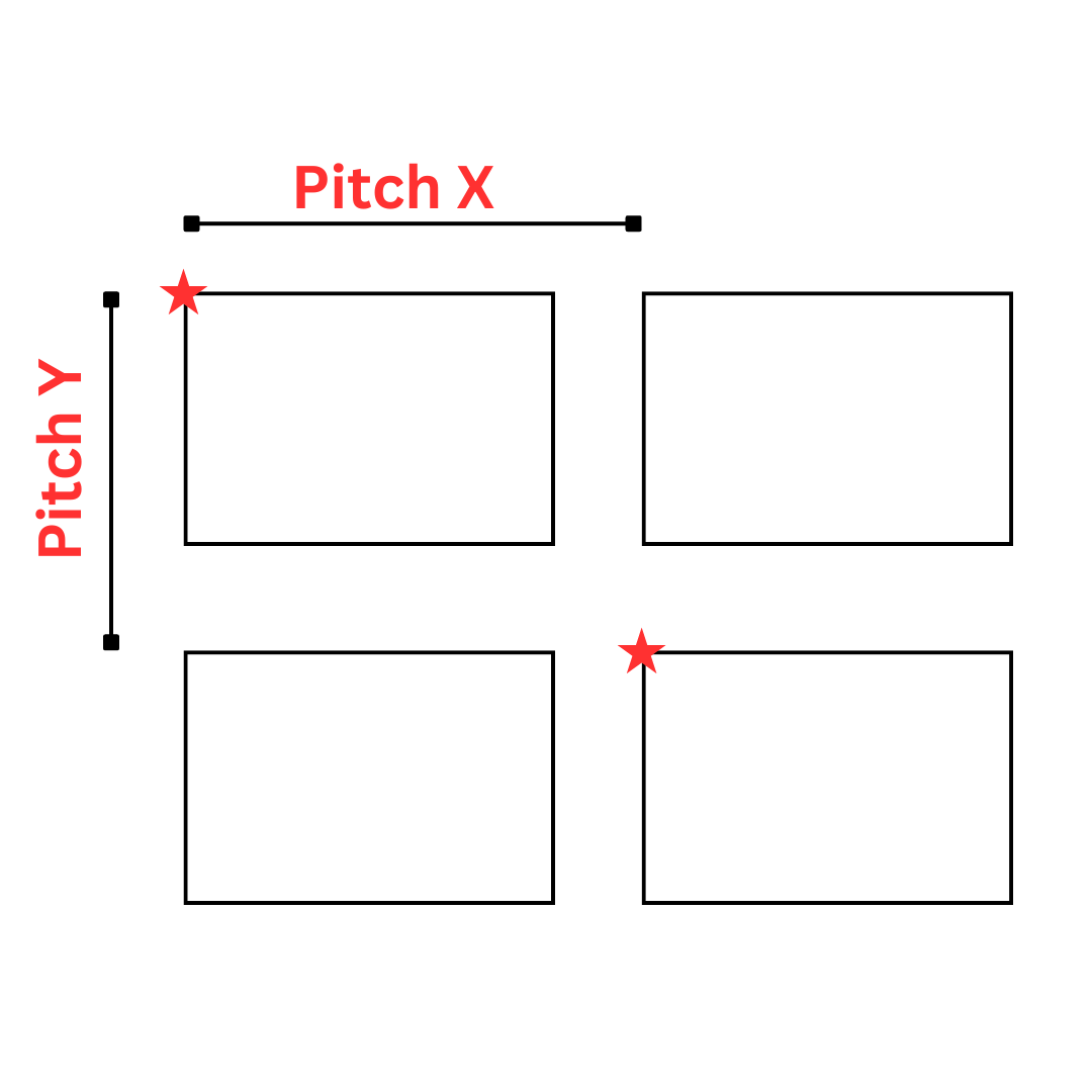
On this patterned wafer, the pitch measurement is x = 4318.22, y = 2007.41.

Input the device measurements into the Die Width and Die Height fields (die and device used interchangeably), and the pitch measurements into the Pitch X and Pitch Y fields.

Verifying and Adjusting Measurements
Creating the device layout is an iterative process. We will now verify the device and pitch measurements, and adjust as needed to ensure the device layout is as accurate as possible.
Verify Device Measurement
First, we’ll check the accuracy of the device measurement by extrapolating exactly one device using the rectangular extrapolation tool – input 1 for rows and 1 for columns to create one device.

An orange box will appear – this is the extrapolated device. Check all four corners of the device to see if the device measurements were accurate. If slightly off, re-measure, clear device list, and extrapolate again.

Verify Pitch Measurement
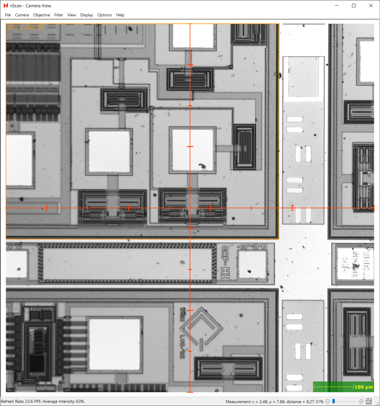
Next, we will measure the accuracy of the pitch measurement. First, clear the device list of any devices from the previous step. Next, use the rectangular extrapolation tool to extrapolate 10 rows and 10 columns.
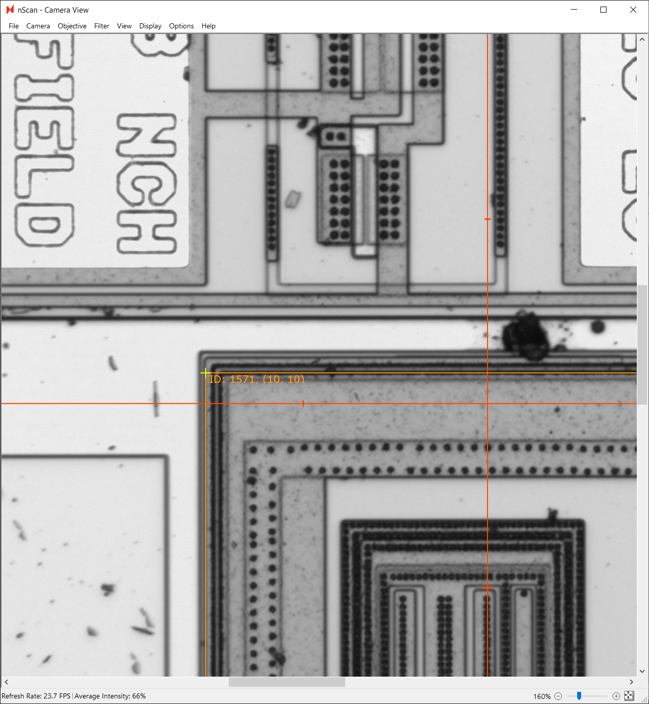
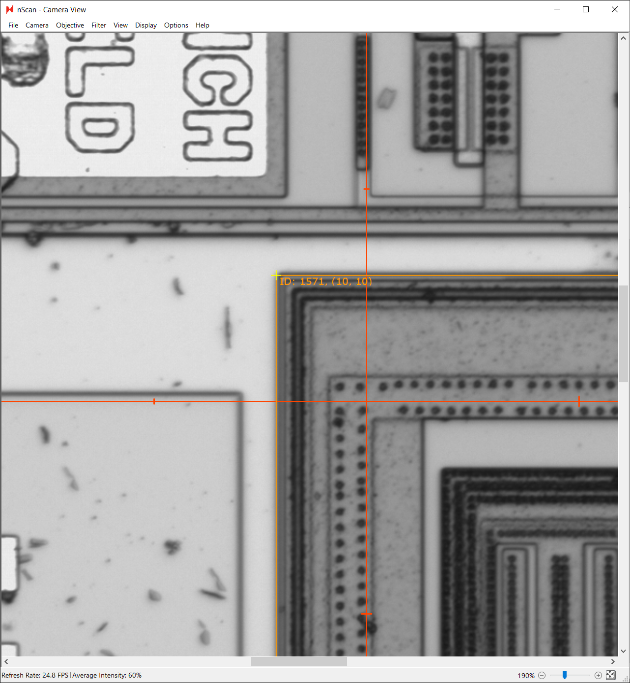
After navigating to the device at row 10, column 10, we see that the orange device boundary is offset from the device. We can click and drag our cursor to use the yellow cursor measurement tool to measure the distance between the device and extrapolated device. In this example, the extrapolated device is offset from the actual device by 3.69 µm in the positive x direction and 10.05 µm in the positive y direction.
Since this offset is the cumulative offset of 10 devices in each direction, we can divide each offset by 10 and subtract them from our original pitch measurement. We will use these new measurements as our pitch values.
4318.22 µm - (3.69 µm / 10) = 4317.85 µm
2007.41 µm - (10.05 µm / 10) = 2006.405 µm
Then, click Clear Device List, extrapolate 10 rows and 10 columns again, and look at the resulting extrapolation. Repeat this step until the extrapolated devices align with the device grid, and enter the final pitch values.
Creating Device Layout
After determining the final die and pitch values, we will use the circular extrapolation tool to create the device layout for this patterned wafer. Make sure the device list has been cleared before this final extrapolation.
The diameter of this wafer is 150 mm, so our Wafer Diameter (µm) field is 150,000 µm. We will apply an Edge Exclusion of 5 mm, or 5000 µm. Then, click Extrapolate to extrapolate devices from the wafer center.
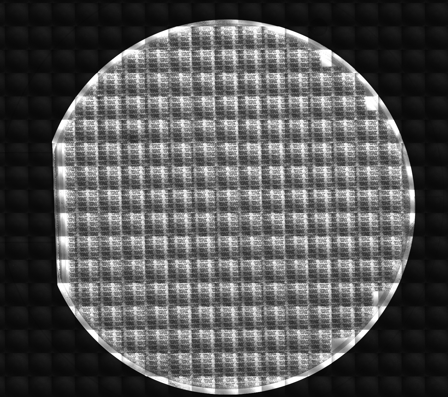
After extrapolating the devices, the nScan - Full Stage View window will populate with all of the devices.

Cleaning Up the Device Layout
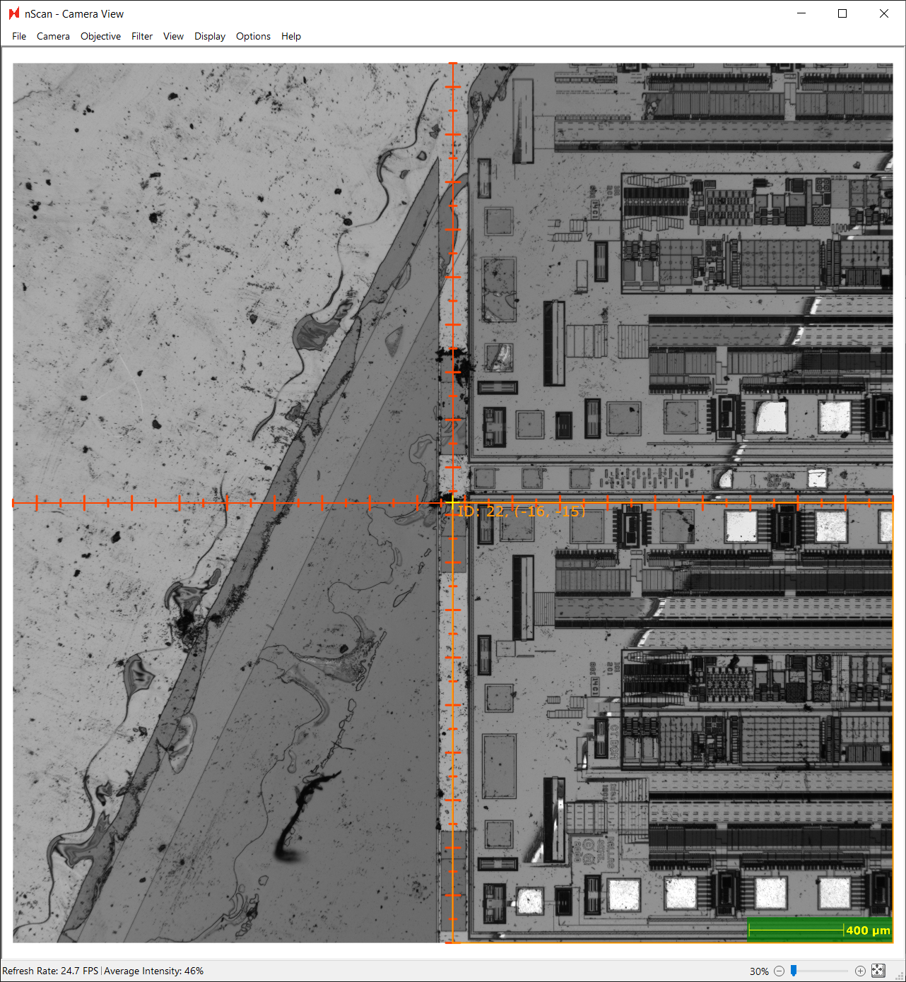
We recommend checking the edges of the device grid to make sure there are no extra extrapolated devices. On this patterned wafer, there is an extra column of extrapolated devices where the wafer’s flat is located. We can delete these excess devices from the device list.

In addition, devices outside of the active device area as seen in the image below should also be deleted from the device list. Any device included in the scan will be used to generate a golden template, which is the standard to which all wafers will be compared to when performing defect detection.
Once the device layout has been cleaned up, click Export Device Layout and save.
Setup Scan
Overview
Running a patterned wafer scan with Device Inspection analysis requires the following prerequisites:
Loading sample onto nSpec stage
Creating an image settings group
Configuring autofocus settings
Creating a north-south-origin alignment
Creating a focus point pattern
Creating a device layout
Once all prerequisites are complete, it’s time to setup a scan with a Device Inspection post-analysis.
The first time a device inspection scan is run, we will create a new “golden template” of the wafer. Refining this golden template often requires running device inspection scans multiple times before getting a golden template that is suitable for use in production.
The golden template represents what a perfect, defect-free device should look like, and is a composite of all scanned device images. Once generated, the template is compared to individual devices to detect defects and deviations from the template.
We will go through the process of creating a golden template for the first time, which often requires running multiple scans to acquire more image data to use for the composite golden template image.
Scan Setup
To open the scan settings dialog, navigate to nScan - Stage View > Scan > Sample…
First, name your sample. Then, under Focus we will choose our autofocus settings and focus point pattern. Under Pattern, we will select the Devices radio button to run a patterned wafer job, and then point to the north-south-origin alignment file and device layout file.
Next, we will setup the Post Scan Analysis. We will run this job and launch a Device Inspection to run after scanning. The three dots next to the Parameters field can be clicked to edit the parameters.
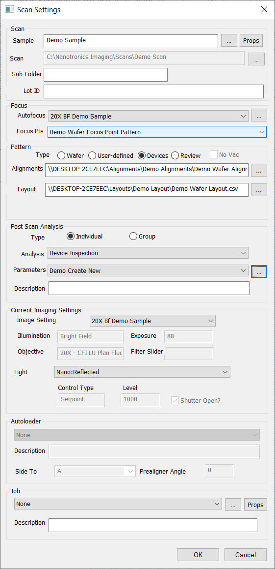
First, we will set the export location and file name of the template by setting the Golden Template parameter to C:/Nanotronics Imaging/Templates/Demo Templates/Demo Wafer Template.
Next, because we are running Device Inspection for the first time for this patterned wafer, select the Create New parameter value under Generate Golden Template to create a new golden template.
Then, in order to reduce the processing power needed, we will change Device Inspection analysis parameter Golden Template Processing Batch Size from -1 to 1. Setting this parameter to -1 will automatically calculate batch size. Changing the batch size parameter to 1 will reduce the amount of processing power needed by restricting the number of images per device to process at a time to 1.
Make sure to click Save As to save your analysis parameter settings.

Lastly, under Current Imaging Settings, point to the image group settings. In this guide, we are running a manual job, but if running a job with an autoloader, make sure to point to relevant autoloader settings. Autoloader settings are setup by Nanotronics service technicians.
Finally, click the three dots in the Job section to save the scan settings as a job. Click OK to start the scan.
Viewing Results of First Scan
After the job completes, the post scan analysis will automatically run. In this example, Device Inspection will analyze the scanned images and launch an nView defect view window which summarizes the findings of the Device Inspection analysis.
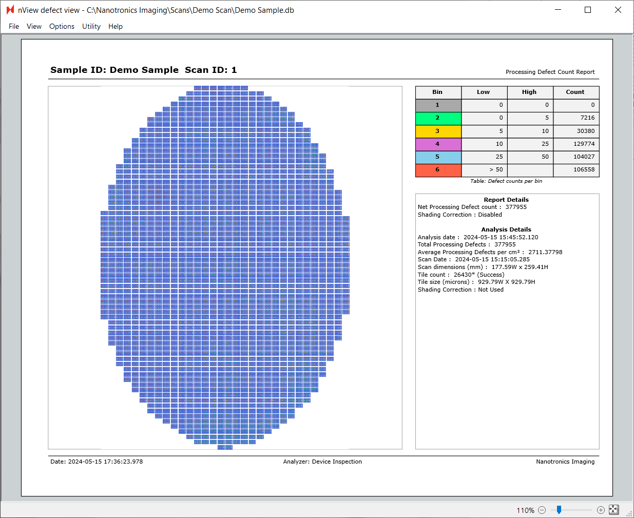
Clicking on the image tiles in Defect View will load an image of the detected defects found during Device Inspection.
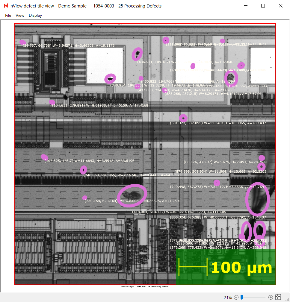
Looking at this tile, we can see that many defects have been detected, but many have not been detected.
To troubleshoot this, we will look at the golden template, which will be at the path that we specified in the Device Inspection analysis parameters at C:/Nanotronics Imaging/Templates/Demo Templates/Demo Wafer Template. Below is one part of the template, which we see is rather blurry, which tells us that our device layout was likely not perfectly aligned everywhere on the wafer.
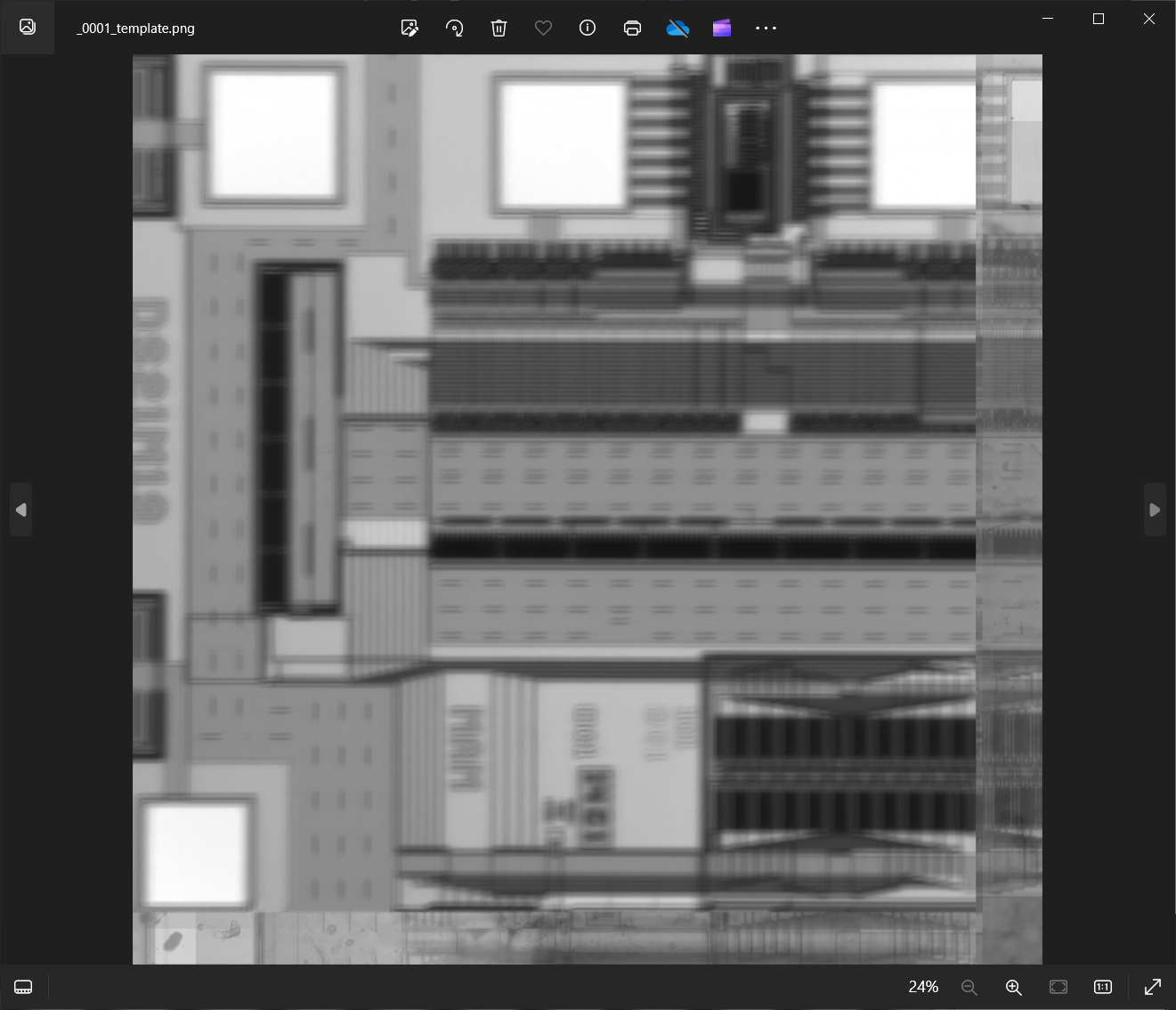
We can compensate for this by increasing the Padding (Pixels) parameter in the Device Inspection analysis parameters dialog from 300 to 700 pixels. This parameter represents the radius nSpec will use to register the template to the scanned image. We will set Generate Golden Template to Create New again.

We will run this scan and analyze again using this new padding value.

Second Scan
After changing the parameters between the first and second scan, the golden template looks much clearer than before. We will now continue improving the golden template with more scans.

Improving Golden Template Through Iterative Scanning
We recommend running jobs with more samples, ideally an entire lot of wafers, to improve the quality of the golden template. For subsequent jobs, we will change the Device inspection analysis Generate Golden Template parameter to Add to Existing.
The number of scanned images needed to improve the golden template quality will depend on the device size (e.g. smaller device size means more device samples per wafer), and also on the desired detection accuracy. We recommend iteratively scanning and checking the Device Inspection analysis results to see if the defects of interest are being captured.
Once the golden template quality is satisfactory, change the Generate Golden Template parameter to Do Not Generate Template when running Device Inspection. This will ensure that the existing golden template is not modified going forward.
Exporting Data
After running a successful analysis, there are several ways of exporting and processing the data obtained.
Manual Export
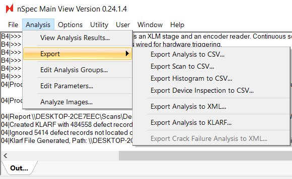
Users can quickly export to CSV, XML, and KLARF formats by exporting from nSpec - Main View > Analysis > Export. Note, that Export Analysis to KLARF… does not export KLARF files with defect images.
Read more about customizing KLARF exports at KLARF Export Properties.
In order to obtain cropped defect images, users should additionally perform a Cropped Images analysis. Details for performing a Cropped Images analysis can be found at Cropped Images Analysis .
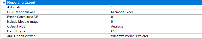
Automatic Export
Users can enable automatic exporting by enabling a program option. The Automatic program option can be found under the Reporting Export subsection. The remaining options should be set based on the desired report type (.CSV, .XML).
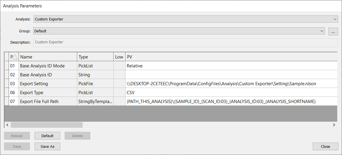
The following image shows an example of an automatic CSV file export setting.
Custom Export
For more flexible exporting options, users can fully customize exports, including custom headers, file format, and extensions, using the Custom Exporter analysis. Custom Exporter’s functionality relies on an input nJson script. The nJson file must be written and configured by Nanotronics Technical Service or Applications Engineers. To request a new custom exporting application that may require assistance, please contact support@nanotronics.ai to request support. To read more about Custom Exporter, see Custom Exporter .