Create Device Layout
Creating a device layout is an important step in preparing to scan a patterned sample, as the layout file contains information about a patterned sample’s device sizes and coordinate locations, as well as the die pitch. Configuring an image setting group, autofocus setting, and north-south-alignment are necessary prerequisites to creating a device layout.
There are three methods for creating a device layout.
Import the device layout from a GDSII file. Note that the origin defined in the GDSII file should be the same as the origin defined in the north-south-origin alignment file.
Translate known device coordinates into an nSpec layout format.
Use nSpec’s device layout creation tool to manually create a layout.
Importing Device Layout from GDSII File
The simplest way to create a device layout file is to simply use an existing GDSII File. Step by step instructions can be found at GDS Layout Creation.
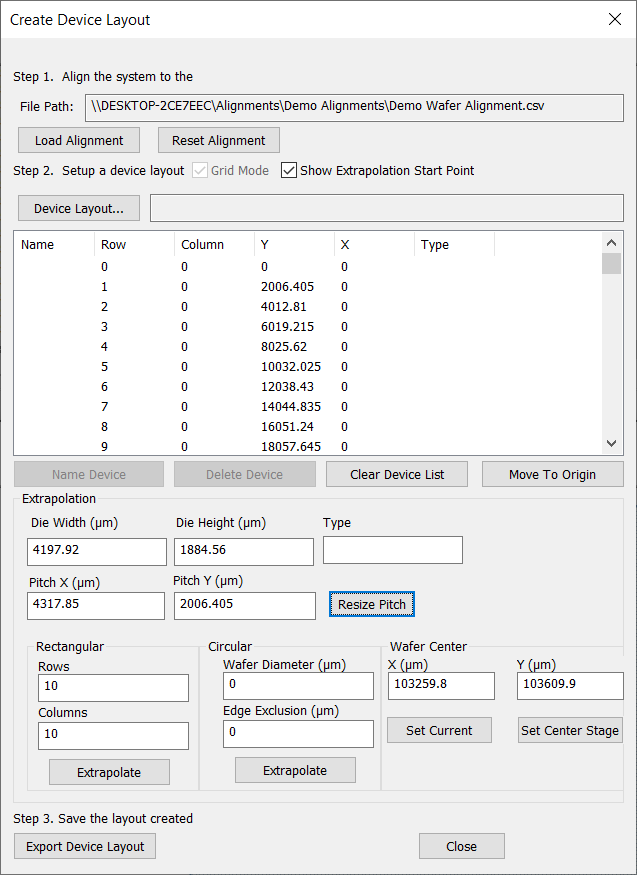
First, open the device layout creation dialog via nScan - Stage View > Scan > Create Device Layout…
Next, load the alignment created during device inspection alignment (aka north-south-origin alignment). The origin defined in the alignment file must match the origin of the GDS file.
After alignment is performed, click the Device Layout… button, then click GDS to import the file. Next, select the appropriate layer to import.
If the import is successful, the device table below will populate with device positions. Click Export Device Layout to finish layout creation.
Creating nSpec Layout from Device Coordinates
Given a set of device coordinates and die pitch values, the nSpec device layout can also be created by formatting the data into a CSV file.
Below is an excerpt of the nSpec device layout CSV file for this wafer. Starting at line 7, each line represents a device’s x and y coordinates, their device coordinates relative to the origin defined during north-south-alignment, the device width and height, name (optional), and type (optional).
Version 1
DiePitchX 4318.168000
DiePitchY 2006.610000
KlarfMode 1
BeginDelimitedListing
Id,X,Y,Xindex,Yindex,W,H,Name,Type
1,-64772.5,-30099.1,-15,-15,4197.92,1884.56,,
2,-64772.5,-28092.5,-15,-14,4197.92,1884.56,,
3,-64772.5,-26085.9,-15,-13,4197.92,1884.56,,
4,-64772.5,-24079.3,-15,-12,4197.92,1884.56,,
5,-64772.5,-22072.7,-15,-11,4197.92,1884.56,,
6,-64772.5,-20066.1,-15,-10,4197.92,1884.56,,
7,-64772.5,-18059.5,-15,-9,4197.92,1884.56,,
8,-64772.5,-16052.9,-15,-8,4197.92,1884.56,,
9,-64772.5,-14046.3,-15,-7,4197.92,1884.56,,
10,-64772.5,-12039.7,-15,-6,4197.92,1884.56,,
11,-64772.5,-10033,-15,-5,4197.92,1884.56,,
12,-64772.5,-8026.44,-15,-4,4197.92,1884.56,,
13,-64772.5,-6019.83,-15,-3,4197.92,1884.56,,
14,-64772.5,-4013.22,-15,-2,4197.92,1884.56,,
15,-64772.5,-2006.61,-15,-1,4197.92,1884.56,,
16,-64772.5,0,-15,0,4197.92,1884.56,,
Manually Create Device Layout
Obtaining the Wafer Center with Bare Wafer Alignment
Before creating the device layout, we will use Bare Wafer Alignment in order to find the location of the wafer center, which is used when extrapolating devices for circular samples.
Create Image Setting Group
Bare wafer alignment is best performed with lower magnification objectives, so we will quickly setup an image setting group named “5x- Demo Bare Wafer Alignment Settings” using the 5x objective. The automatic focus settings will not be used in bare wafer alignment, so it’s not necessary to adjust them.

Running Bare Wafer Alignment
Next, we will run bare wafer alignment. Navigate to the dialog via nScan - Full Stage View > Bare Wafer Alignment > Start Wizard…
Most default settings run well, but we will decrease the Pixels in Line parameter from the default of 150 to 80.
This parameter depends on the size and shape of the fiducial, as it determines the number of pixels used to find the wafer fiducial. If the value is too high, it may not detect the fiducial. If it is too low, it may falsely detect other structures on the wafer edge as the fiducial.
Next, we will set Wafer Fiducial to Single Flat and set Image Settings to the “5x- Demo Bare Wafer Alignment Settings”.
Under Wafer Trace Settings, we will increase the Edge Trace Speed to 20,000 µm/s to increase the speed of the bare wafer alignment process. We will also note the location of the wafer fiducial by clicking the “W”.
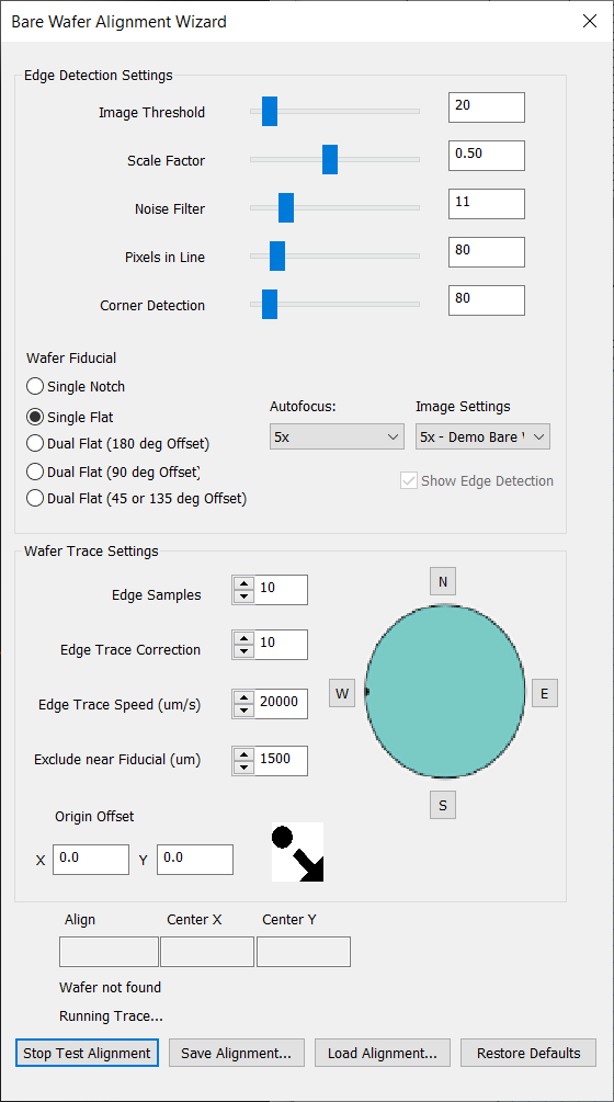
After setting all of these parameters, we will Test Alignment. After the alignment is performed, the Center X and Center Y fields will populate with the wafer center values found during alignment.
For this wafer, the center is at (103,259.8, 103609.9). Write these values down for the following device layout creation step. Additionally, you will see all the found points in nScan - Full Stage View.
Make sure to click Save Alignment…

Starting Device Layout Creation
After finishing bare wafer alignment, open the device layout creation dialog via nScan - Stage View > Scan > Create Device Layout…
First, load the alignment created during device inspection alignment (aka north-south-origin alignment). The system will perform alignment.
Next, input the wafer center values found during bare wafer alignment. Set Current will automatically input the current stage position as the wafer center values.
We will keep the Grid Mode box checked, because the patterned wafer we are scanning has uniform pitch X and Y values throughout the wafer.
Measuring Device Size
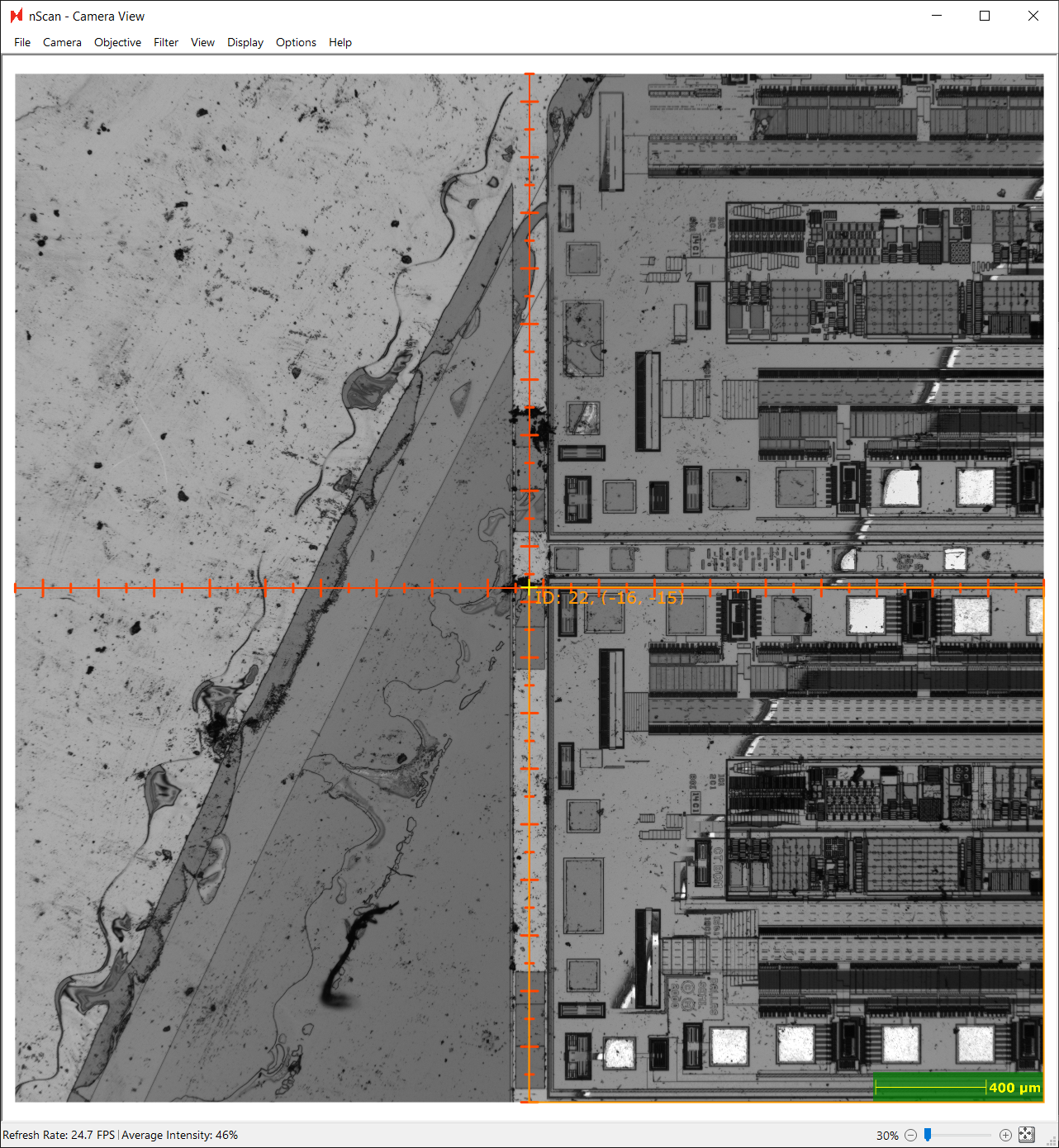
Next, we will use the Long Distance Measurement Tool found at nScan - Camera View > View > Long-Distance Measurement to measure the device size. Selecting the measurement tool changes the cursor in nScan - Camera View to a red target.
To measure the device size, click the top left corner of any device, then without clicking the screen, navigate to the bottom right corner of the same device and click the bottom right corner. We recommend using the zoom feature to be able to choose the measurement locations as precisely as possible.
Once clicking these two points, a measurement will appear in the bottom right corner of the nScan - Camera View screen. In this example, x = 4197.92, y = 1884.56. The measurement values are in µm.

Measuring Pitch Size
Next, we will measure the pitch size. Pitch for a given axis is the distance between the same point on adjacent devices. We will use the Long-Distance Measurement tool again to measure the pitch X and pitch Y.
The quickest way to measure both pitch X and Y is to measure between the same point on two devices that are directly diagonal to one another. In the diagram below, these measurement points are marked with stars.
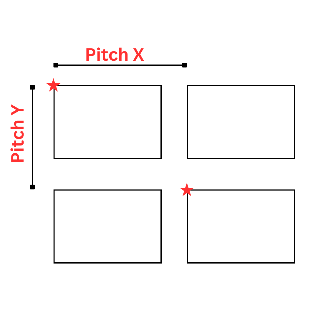
On this patterned wafer, the pitch measurement is x = 4318.22, y = 2007.41.

Input the device measurements into the Die Width and Die Height fields (die and device used interchangeably), and the pitch measurements into the Pitch X and Pitch Y fields.

Verifying and Adjusting Measurements
Creating the device layout is an iterative process. We will now verify the device and pitch measurements, and adjust as needed to ensure the device layout is as accurate as possible.
Verify Device Measurement
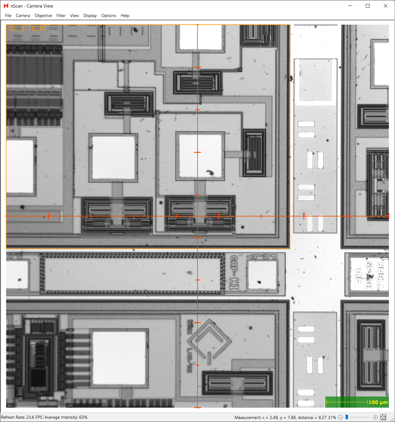
First, we’ll check the accuracy of the device measurement by extrapolating exactly one device using the rectangular extrapolation tool – input 1 for rows and 1 for columns to create one device.

An orange box will appear – this is the extrapolated device. Check all four corners of the device to see if the device measurements were accurate. If slightly off, re-measure, clear device list, and extrapolate again.

Verify Pitch Measurement
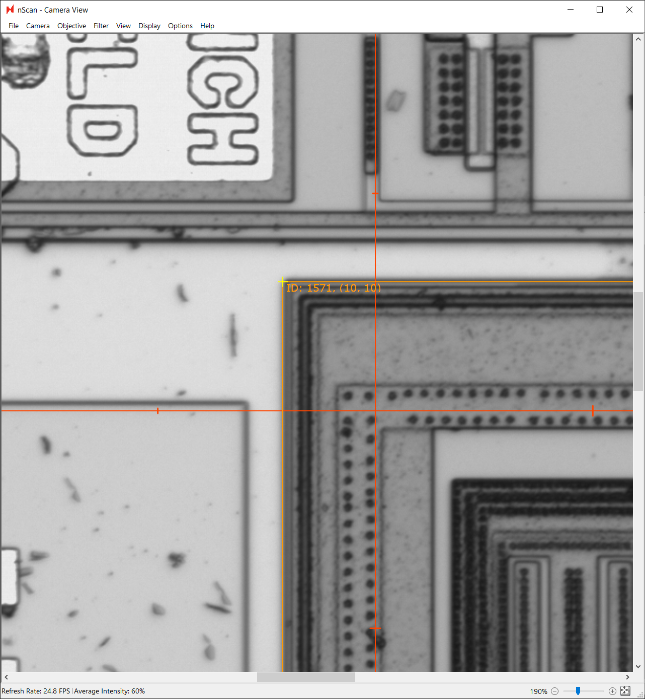
Next, we will measure the accuracy of the pitch measurement. First, clear the device list of any devices from the previous step. Next, use the rectangular extrapolation tool to extrapolate 10 rows and 10 columns.
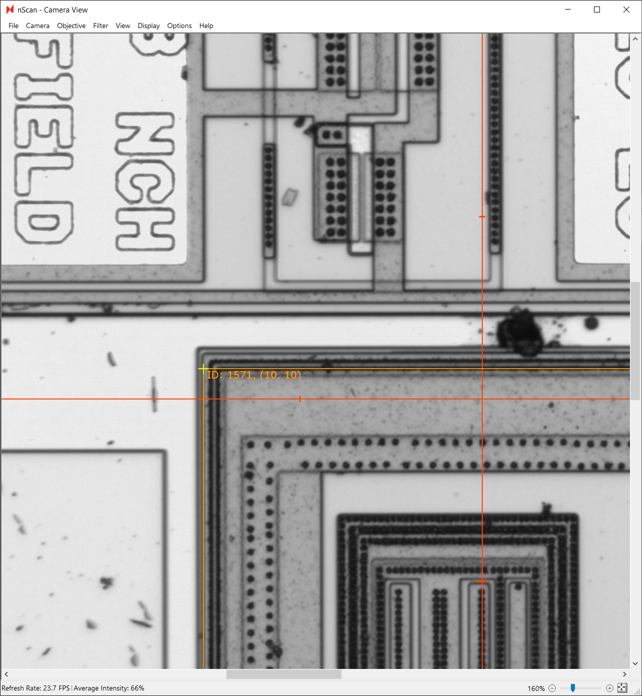
After navigating to the device at row 10, column 10, we see that the orange device boundary is offset from the device. We can click and drag our cursor to use the yellow cursor measurement tool to measure the distance between the device and extrapolated device. In this example, the extrapolated device is offset from the actual device by 3.69 µm in the positive x direction and 10.05 µm in the positive y direction.
Since this offset is the cumulative offset of 10 devices in each direction, we can divide each offset by 10 and subtract them from our original pitch measurement. We will use these new measurements as our pitch values.
4318.22 µm - (3.69 µm / 10) = 4317.85 µm
2007.41 µm - (10.05 µm / 10) = 2006.405 µm
Then, click Clear Device List, extrapolate 10 rows and 10 columns again, and look at the resulting extrapolation. Repeat this step until the extrapolated devices align with the device grid, and enter the final pitch values.
Creating Device Layout
After determining the final die and pitch values, we will use the circular extrapolation tool to create the device layout for this patterned wafer. Make sure the device list has been cleared before this final extrapolation.
The diameter of this wafer is 150 mm, so our Wafer Diameter (µm) field is 150,000 µm. We will apply an Edge Exclusion of 5 mm, or 5000 µm. Then, click Extrapolate to extrapolate devices from the wafer center.
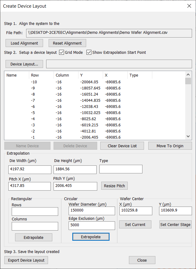
After extrapolating the devices, the nScan - Full Stage View window will populate with all of the devices.

Cleaning Up the Device Layout
We recommend checking the edges of the device grid to make sure there are no extra extrapolated devices. On this patterned wafer, there is an extra column of extrapolated devices where the wafer’s flat is located. We can delete these excess devices from the device list.

In addition, devices outside of the active device area as seen in the image below should also be deleted from the device list. Any device included in the scan will be used to generate a golden template, which is the standard to which all wafers will be compared to when performing defect detection.
Once the device layout has been cleaned up, click Export Device Layout and save.