
nSpec v0.22.1.5 External Release Notes
nSpec Version 0.22.1.5
Release Date:
Documentation Updated:
Major Features: Wafer Values Written to Database
Overview
This patch includes a change to how certain wafer properties are written to in the database. Previously, those values were obtained manually via job properties, but now are automatically calculated and written to the database when performing a Bare Wafer Alignment.
Upgrading to v0.22.1.5
Library Update Not Required
If upgrading from a version more than 1 release prior, please reference all intermediate release notes for upgrade steps for each version.
New Features
Highlights
NSPEC-7116: Values Calculated from Bare Wafer Alignment Written to Database
With this update, certain wafer properties measured and calculated during Bare Wafer Alignment will be automatically written to the database. These property values can also be manually input as job properties, and manual inputs will overwrite the values obtained from running Bare Wafer Alignment in the database.
Running Bare Wafer Alignment will calculate and write the following values to the database.
Scan Property | Description |
|---|---|
SampleOrientationMarkType | Notes the wafer fiducial type, Notch or Flat. *When using the autoloader and performing a bare wafer alignment, if a flat is not found, the scan property value is automatically determined to be a Notch. If Bare Wafer Alignment is not performed at all, the value is NA. |
OrientationMarkLocation | Notes the orientation of the wafer fiducial, North, South, East or West. If there is more than one orientation mark, this value will mark the orientation of the larger of the two orientation marks (e.g. if there are two flats, this value denotes the major flat location.) If in the rare case there are multiple marks of the same size, this value denotes the first mark found during alignment. |
WaferCenterX | X axis value that marks the center of the wafer, relative to the stage origin (top left corner). |
WaferCenterY | Y axis value that marks the center of the wafer, relative to the stage origin (top left corner). |
OrientationMarkLength
| Micron measurement of each flat. If there are multiple marks, the value written to the database will be a comma separated value of the mark lengths in descending length. |
For more information on performing a Bare Wafer Alignment, see the Appendices section.
New Features Changelog
Appendices
Bare Wafer Alignment
Overview
nSpec supports alignment of bare wafers. The Bare Wafer Alignment uses an automatic fiducial detection algorithm to find the angle of any wafer, bare or patterned, relative to the stage. The alignment file generated using the Bare Wafer Alignment Wizard is an optional, but highly recommend input to the Scan Settings dialog.
Enabling Bare Wafer Alignment in Scan Settings
The Alignments field for Wafer patterns in the Scan Settings dialog can accept both Device Inspection Alignment files (.csv) and Bare Wafer Alignment files (.json).
Alignment will be enabled if this field has a valid alignment file.
Alignment will be disabled if this field is left blank.

Alignments field in Scan Settings Dialog
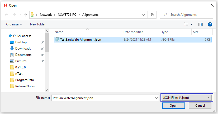
Bare Wafer Alignment (JSON) file selection
Prerequisites for Creating a Bare Wafer Alignment File
Prior to creating a Bare Wafer Alignment file, do the following:
Place a representative wafer on the stage.
Create an image settings group with low magnification (i.e., 1x, 2.5x, or 5x should all work).
Create an autofocus group with Use F-stop set to 0.
Navigate to the wafer’s fiducial (i.e., flat’s corner or notch) so that it is centered in the live view.
Creating a Bare Wafer Alignment File
To create a Bare Wafer Alignment file, navigate to the Bare Wafer Alignment Wizard through Stage View > Scan > Bare Wafer Alignment > Wizard.
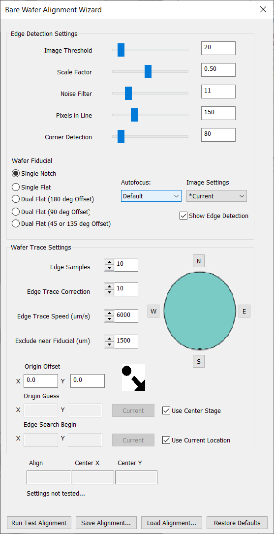
The Bare Wafer Alignment Wizard will appear, and the live view will automatically have Edge Detection enabled. When enabled, Edge Detection will display the following highlights in the live view:
Color | Description |
|---|---|
Gray | Wafer area |
Black | Stage area |
Green | Wafer edge |
Blue | Other contours |
Yellow | Cross indicates detection of a fiducial’s corner |
Red | Indicates how lines are detected |

The goal of this alignment setup is to optimize the settings in the Bare Wafer Alignment Wizard so that only the corners of the target fiducial have yellow crosses on them. You can then click Run Test Alignment to test the assigned settings. Once satisfied, you can click Save Alignment… to save the alignment.
Bare Wafer Alignment Wizard Settings
Edge Detection Settings
Setting | Description | Recommendation |
|---|---|---|
Image Threshold | Determines which part of the image is wafer vs stage. | 20 is usually good. |
Scale Factor | Determines scaling of the image for processing. | Lower is faster but can create reduce precision. |
Noise Filter | Applies a blur filter to reduce noise. | Use this and Smoothing to remove excess contours and make sure the edge of the |
Pixels in Line | The number of pixels used to find the line. | If the fiducial isn’t being found reliably, lower this value. |
Corner Detection | The distance allowed for the corner detected to be from the edge. | Keep as low as possible. |
Minimum Angle | The minimum angle between red lines that identifies a corner. | For notch wafers, 35° is usually a good choice. |
Autofocus | Autofocus group to use when alignment starts. | |
Image Settings | Image settings to use during alignment. |
Wafer Trace Settings
Setting | Description | Recommendation |
Edge Samples | Number of samples to take along | More will be more accurate but slower. |
Edge Trace Correction | Angle the stage movement takes when moving to the next sample. | Adjusting this can help track the edge better. |
Edge Trace Speed (µm) | Distance the trace will move at each stage instruction. | Lower will be slower, but more reliable. For nSpec systems with higher FPS, this can be higher. |
Exclude near Fiducial (µm) | Distance a point must be from the fiducial to be used for center | Increase if the fiducial is being included in edge calculations. |
Origin Offset (µm) | Applies an offset to the origin point defined in a layout file. | |
Origin Guess (µm) | Origin guess is the expected sample center. | Setting this parameter is helpful if nSpec has trouble finding the sample on the stage at the start of the alignment process. |
Edge Search Begin (µm) | nSpec will begin searching for the edge of the wafer to begin bare wafer alignment at this position. | Setting this parameter is helpful if nSpec has trouble finding the sample on the stage at the start of the alignment process. |
Wafer Alignment | Four buttons N, S, E, W for selecting where the fiducial is supposed to be aligned. | Align angle result will be the rotation needed to align the wafer with that point. |
Measurements Taken During Bare Wafer Alignment
Certain wafer properties measured and calculated during Bare Wafer Alignment will be automatically written to the database. These property values can also be manually input as job properties, and manual inputs will overwrite the values obtained from running Bare Wafer Alignment in the database.
Running Bare Wafer Alignment will calculate and write the following values to the database.
Scan Property | Description |
|---|---|
SampleOrientationMarkType | Notes the wafer fiducial type, Notch or Flat. When using the autoloader and performing a bare wafer alignment, if a flat is not found, the scan property value is automatically determined to be a Notch. If Bare Wafer Alignment is not performed at all, the value is NA. |
OrientationMarkLocation | Notes the orientation of the wafer fiducial, North, South, East or West. If there is more than one orientation mark, this value will mark the orientation of the larger of the two orientation marks (e.g. if there are two flats, this value denotes the major flat location.) If in the rare case there are multiple marks of the same size, this value denotes the first mark found during alignment. |
WaferCenterX | X axis value that marks the center of the wafer, relative to the stage origin (top left corner). |
WaferCenterY | Y axis value that marks the center of the wafer, relative to the stage origin (top left corner). |
OrientationMarkLength
| Micron measurement of each flat. If there are multiple marks, the value written to the database will be a comma separated value of the mark lengths in descending length. |
WaferMeasuredDiameter | Micron measurement of sample’s diameter. Note: The diameter of the sample’s major axis is measured. |