nSpec v0.22.0.0 External Release Notes
Release Date:
Documentation Updated:
Major Features: Dislocation, Wafer Flatness, Surface Scattering Analyzers
Overview
This is one of the most impactful releases for nSpec in the last several years, and we’re very excited to share some long-awaited new features with you. Improvements included in this version fall into a few different categories:
New Analyzers (Dislocation, Surface Scattering, Flatness, Defect Cropping)
Reporting (Defect Annotations, Exclusion Zones, Histogram Rendering, Legibility, Zoom)
Alignment (Autoloading non-standard wafer sizes, Device Inspection alignment bug fixes)
Core Stability (Much Faster Initialization, GEM stability fixes)
v0.22.0.0 introduces a totally revamped etched Dislocation Defect Analyzer that is backed by the latest Nanotronics machine learning intelligence. It is highly configurable, completes in seconds, and has dramatically improved accuracy compared to our legacy dislocation defect solutions. v0.22.0.0 also introduces the all new Surface Scattering Analyzer, a Cropped Images Analyzer, and a Flatness Report in nView to help you understand sample flatness and scan-time focus performance.
Upgrading to v0.22.0.0
Required Library Update!
To upgrade from previous versions, a few things need to be checked:
Run the nanotronics-libraries-installer-v22_0-20220314.exe installer to update 3rd party libraries related to the new Flatness Analysis. Contact technical service if you are missing this installer.
Run all upgrading steps for versions v0.21.0.0 and v0.21.1.0 - we recommend running all installers for major builds of nSpec between the previous version and the target version
Major Enhancements
Surface Scattering Analysis
Overview
A common request from customers is to be able to measure the surface roughness of a sample. Surface roughness is closely related to haze, which is the optical phenomenon resulting from surface roughness. This analysis is also commonly referred to as “haze analysis”.
nSpec’s Surface Scattering Analysis works by measuring the intensity of scattered light when scanning a sample in Darkfield Illumination mode. This analyzer has two reporting options:
An interactive Surface Scattering report within nView.
A PNG summary export and CSV data file.
Input Scan Requirements
Darkfield Illumination
This analyzer requires the target scan to have been captured in Darkfield Illumination mode. Darkfield Illumination captures more meaningful topographical data because of the oblique angle of incidence utilized in darkfield imaging.
Bare Wafer Samples
Surface Scattering Analysis can theoretically be performed with both bare and patterned wafers, however, performing the analysis on a patterned wafer may not generate meaningful results or useful data, so it is highly recommended for use to analyze bare wafers only.
Analysis Parameters
There are only two analysis parameters for Surface Scattering Analysis. For the most part, the two parameters don’t need to be touched.
Export Map Bins determines the number of bins used to display haze data in nView.
Export JSON is used to export analysis results to a JSON file.
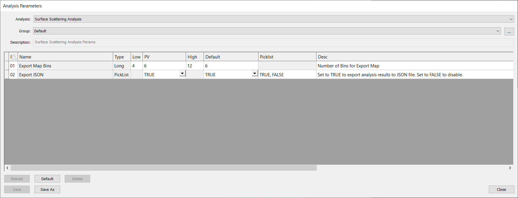
Analysis Parameters Dialog
Reporting
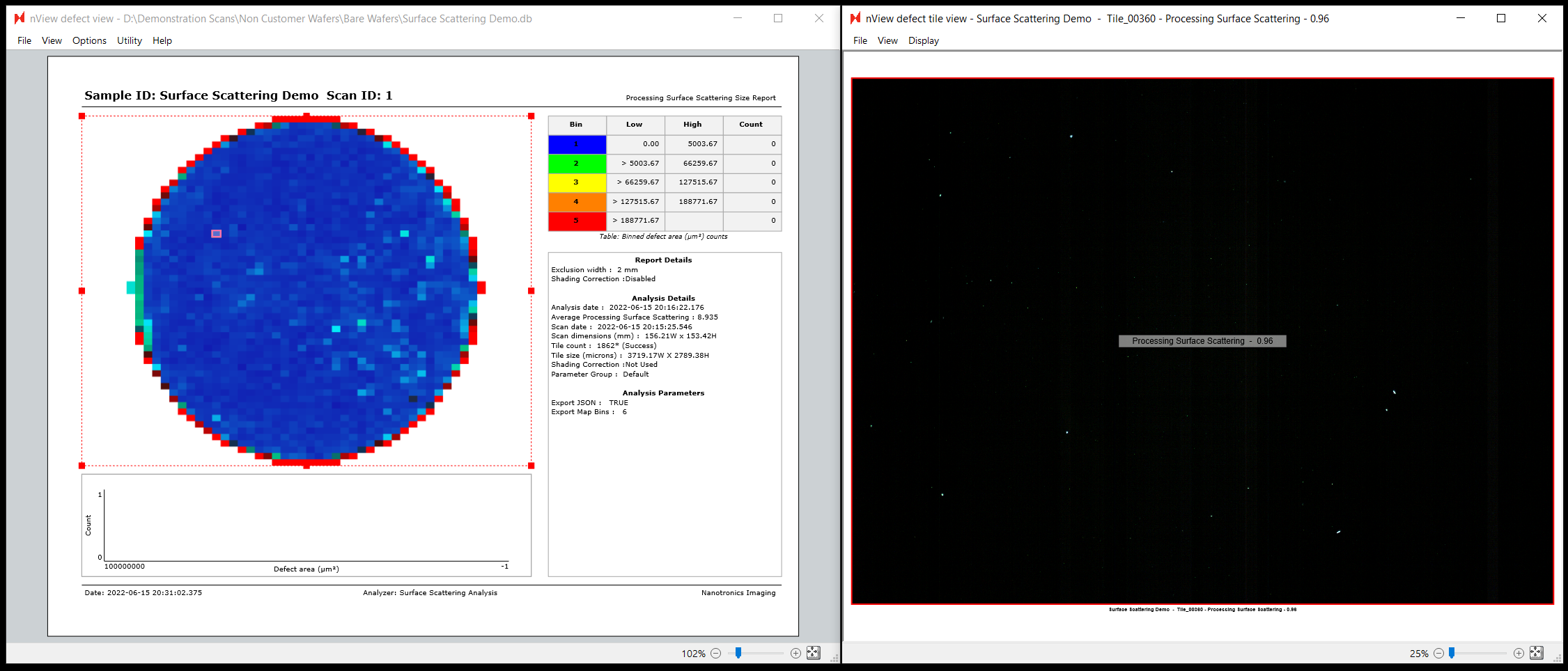
Interactive nView Report
To view the surface scattering report within nSpec, you will need to open the Image Property Report. This should open by default when viewing results for the Surface Scattering Analysis, however you may then need to select either Map or Merged mode to see the results on the sample map, if that mode is not set as your reporting default.

To view the value for a specific image tile, simply click on the target image and view the value printing in the middle of the tile to the right.
The surface scattering value is a unitless measurement, and correlates with how much pixel-scale scattering there is. It is roughly equivalent to an average brightness of background pixels in a darkfield scan. The higher the number, the more haze is present.
Exports
A number of exports will also be generated by default for this analysis and saved to the scan analysis folder.
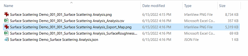
This includes a PNG report visualizing the surface scattering values across the sample:

As well as a CSV report with the same information in the following columnar form:
Row | Column | X (Microns) | Y (Microns) | Surface Scattering Value |
26 | 0 | 22122.7 | 100859 | 6.294322491 |
27 | 0 | 22122.7 | 103649 | 6.334250689 |
31 | 1 | 25841.9 | 114806 | 9.976365487 |
The analysis parameters also provide an option to export the standard JSON file that all nSpec analyzers generate, however since this analysis does not produce defect-type results this JSON file will be mostly empty and not interesting to consume externally. We recommend instead focusing on the surface scattering PNG and CSV exports, or using the interactive report within nView.
Flatness Report & Bow Analysis
Overview
The Flatness Report is an addition to nView that renders the surface of any nSpec scan. This can help you understand the surface topology of your samples. This feature can also help you troubleshoot autofocus settings by allowing you to visualize your sample surface when a Surface Prediction algorithm is not characterizing surface topology optimally. This is especially true if you use this in tandem with the new feature to save autofocus images during the scan.
The Flatness Report is available for all scans that included an autofocus step that generated a Predictive Focus map.
Note: previous versions of this documentation equated “flatness” to “bow”, which is inaccurate. Flatness and bow measurements are not equivalent terms. For more information about the differences between the terms, we recommend reading the definitions in http://www.mast-tech.com.tw/semi-definition.pdf.
Scanning
The Flatness Report will be available for any scan that used a surface prediction algorithm.
Reporting
Accessing the Report within nView
In addition to the Flatness Report now available to all scans, nSpec now also supports a special scanning mode that will allow you to perform a Flatness Analysis without vacuum so that a measurement can be performed without the stage vacuum pulling the sample flat during the measurement.
To utilize, simply check the new No Vac option checkbox on the Jobs dialog:

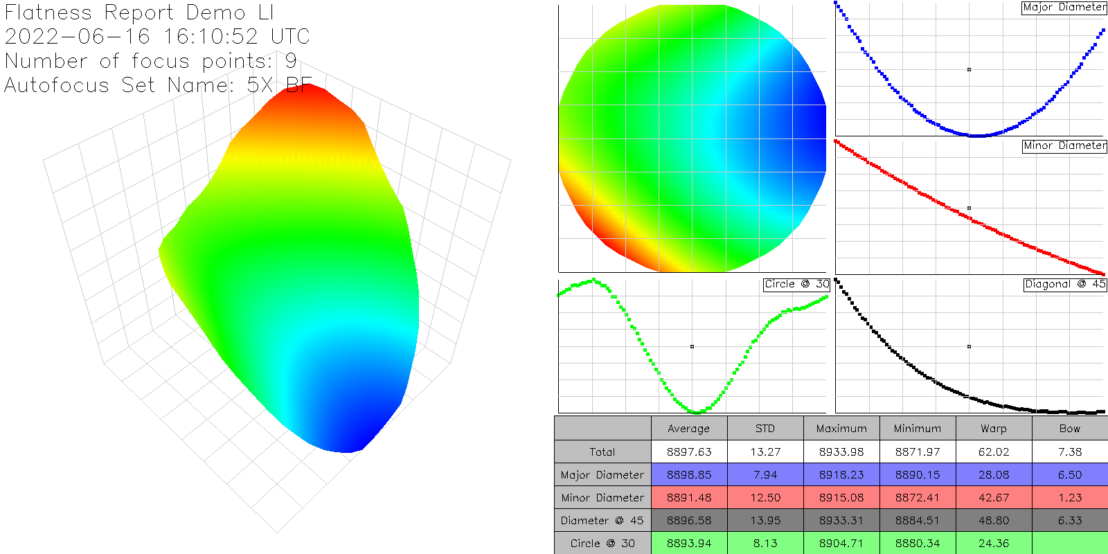
To find the Flatness Report for a scanned wafer, all you need to do is navigate to the new Flatness Report option (ctrl+6) when viewing results in nView:
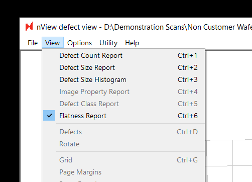
On the left the report shows an interactive 3-dimensional rendering of the sample. On the right, the same data is rendered from a top-down perspective. The scale bar in the center displays the nSpec stage Z coordinates corresponding to a given color on the two maps.
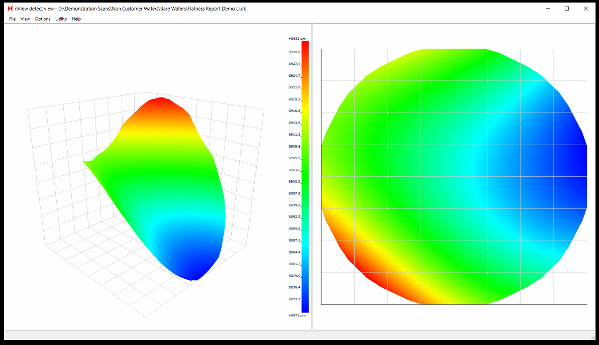
Note: when viewing results in nView, the Flatness Report values includes any potential tilt in the stage. However, the values in the exported Flatness Report PNG file are corrected for tilt.
Exporting a PNG Report
Since the Flatness Report doesn’t require an explicit analysis to be performed and is extended to all scans, triggering a Flatness Report is a bit different from other exports in nSpec. Elsewhere you have analysis parameters to control JSON, CSV, and image exports.
To export a full flatness report, you need to use a new Job Property:
Name | Value Type | Description |
|---|---|---|
ExportFlatnessReport | Bool (TRUE, FALSE) | Enable flatness report export after scan succeeds |
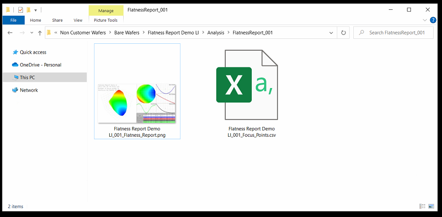
After the scan is completed, a folder will be added in the location dictated by the ReportExport program option.
This folder will be named FlatnessReport_<Scan_ID> (ex. FlatnessReport_001).
Within this folder will be two files:
<Sample ID>_<Scan_ID>_Flatness_Report.png
<Sample_ID>_<Scan_ID>_Focus_Points.csv
Since our stages have their Y axis flipped (0,0 is the TOP left of the stage when facing the nSpec machine) the values will appear flipped:
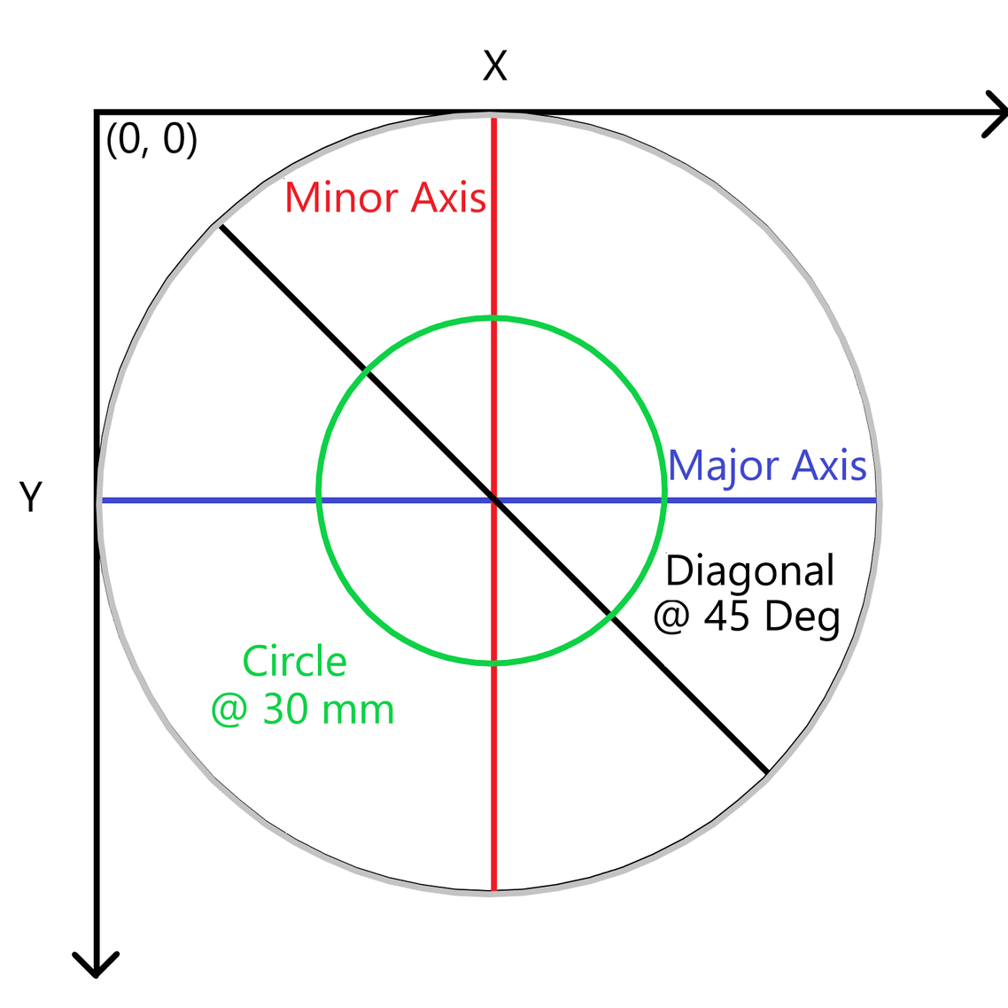
The image export has the following information, corrected for any potential tilt in the stage:
3D orthogonal view (scatter plot)
Top-down view
Major axis slice
Minor axis slice
45 degree slice
30 mm ring slice (hardcoded 30 mm)
Table of calculations: Average value, Standard deviation, Min, Max, Bow, Warp
An example Flatness Report PNG:
As well as a raw and simple CSV export of the focus points collected during the scan:
X (µm) | Y (µm) | Z (µm) |
|---|---|---|
103349.9 | 133045 | 8900.789 |
61099.9 | 133045 | 8913.055 |
61099.9 | 90795.02 | 8907 |
61099.9 | 48545.02 | 8933.602 |
103349.9 | 48545.02 | 8905.148 |
103349.9 | 90795.02 | 8890.289 |
145599.9 | 90795.02 | 8876.977 |
145599.9 | 48545.02 | 8891.602 |
145599.9 | 133045 | 8884.781 |
Focus Point Pattern Editor
Overview
This is a major upgrade to our focus point pattern generation interface. This upgrade includes new abilities to:
Create aligned focus patterns
Create Circular patterns
Easily Create Square/Rectangular patterns
One major difference is that all patterns extrapolate from the current position as the center point of the pattern instead of the top left point
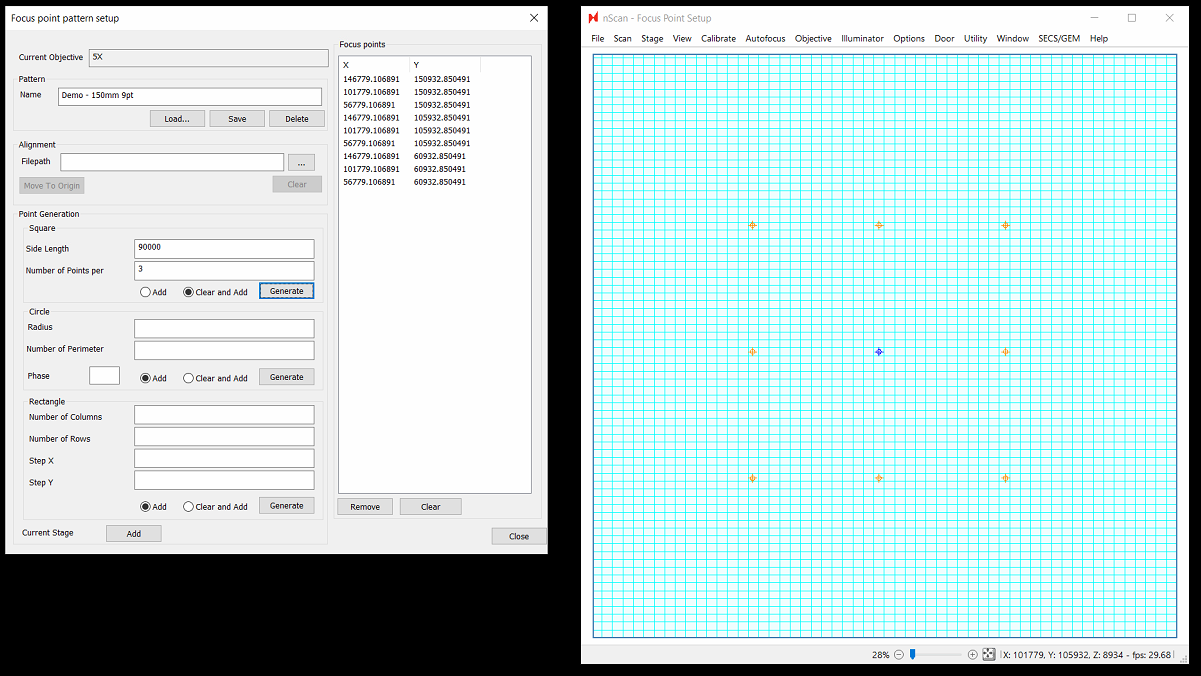
Using the newly available pattern creation options, almost any pattern you imagine can be created. Use responsibly! More focus points will come at the cost of throughput, so in general we still recommend starting with a square 9 point pattern paired with LI predictive focus interpolation. Let us know what patterns & predictive focus algorithm works best for your wafers, as this will help us further improve focus quality in future releases.
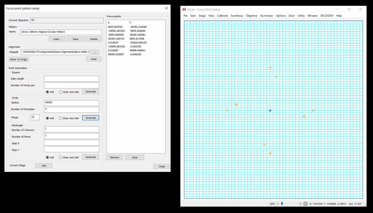
Aligned Focus Patterns
Historically all nSpec focus patterns were defined in terms of stage coordinates. With aligned focus patterns, coordinates are defined relative to the aligned origin of your sample. This can useful because it guarantees that focus points will be positioned over the same part of the sample on every scan even if there is small placement variation on the physical stage. This applies both for Bare Wafer Alignments as well as Device Inspection style alignments. For bare wafer alignments, the coordinates will be relative to the calculated center of the wafer. For Device Inspection alignments, coordinates are relative to the origin point defined in the alignment file (which is not necessarily the center of the wafer).
To configure an aligned focus pattern, simply load an alignment in the Focus point pattern setup dialog.
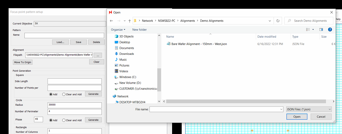
You may need to select JSON files at the bottom right to view your alignment file
Once an alignment has been selected, the alignment will be performed. This means that you will need a wafer / sample loaded on to the stage to perform the alignment successfully.
Once complete, you will have the option to use the Move to Origin button, which will send your current position to the origin found during the alignment. This is useful as a starting position for completing the focus pattern setup.
New Patterns & Concepts
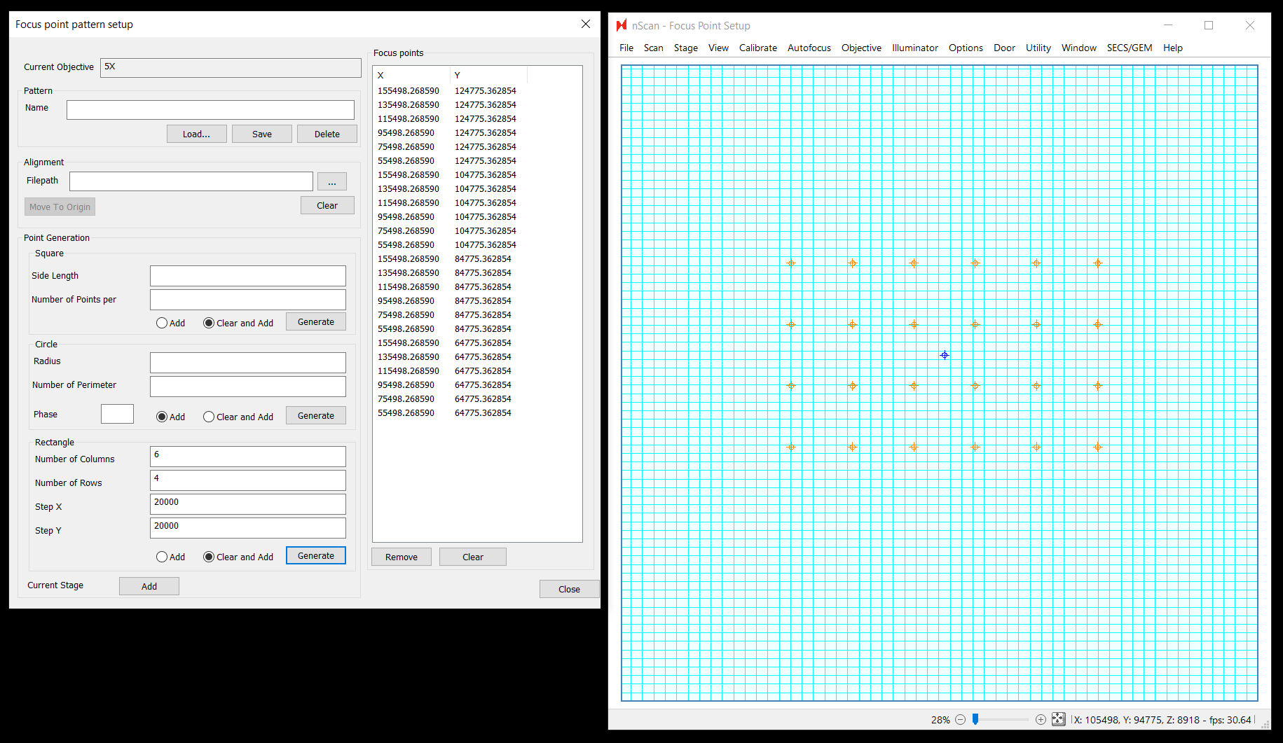
Circular Patterns
Circular patterns have finally arrived for nSpec! This pattern could be helpful if you wish to use a very dense canvas of focus points paired with a triangular predictive focus algorithm. To se this up, move to the center of the stage (or the origin if using an aligned pattern - this would require your job to also perform some form of alignment). Then set a radius and number of points to apply along that circumference. In the below example, 10 points were added at two separate radii (70,000 microns from the origin, and 30,000 microns from the origin:

Phase is a new option as well. Phase will rotate points relative to other phases. In the below example, a phase of 10 degrees was applied to the points with a smaller radius. Applying a positive phase rotates in the clockwise direction:
Square & Rectangular Patterns
In the Square section, extrapolation applies with a total side length, adding the specified number of points along the edges, and filling in the square pattern. Extrapolation occurs from the center point for both even and odd number of points along the side:

In the Rectangle section, extrapolation applies the X and Y step between points with the columns and rows specified. Extrapolation still occurs from the center point:
Dislocation Analyzer
The Dislocation Defect analyzer uses a trained AI model to identify and classify defects found in images of a scan. This article provides an overview about dislocation defects and how the Dislocation Defect analyzer works in nSpec.
Overview
Dislocations are line defects that exist in the crystal structure of metals. More information about dislocations can be found here.
The goal of the Dislocation Defect analyzer in nSpec is to find and classify dislocation defects on etched silicon carbide (SiC) substrates. Specifically, the Dislocation Defect analyzer does the following to find and classify dislocations in a provided image:
Find irregular shapes and patterns
Determine if that shape or pattern is a defect
Classify that defect using a trained AI model
Historically, we have had to generate entirely unique builds of nSpec to deploy different flavors of the Dislocation Analyzer at customer sites. This has caused a problematic divergence of features and functionalities available to these customers over time, sometimes even across different nSpec systems at the same customer. This is the most important step towards enabling these customers to get back on the main branch of software improvements, while also dramatically improving our core Dislocation Defect Analyzer. This work also sets the stage for easier customer-specific customization of our dislocation analyzer moving forward.
For complete instructions on how to train and configure the new Dislocation Analyzer, please reach out to us at support@nanotronics.ai
Dislocation Classification Types
This article uses a sample set of dislocation classifications:
These are only some types of dislocations - there are many more. The Dislocation Defect analyzer can classify defects using the provided sample classifications above or use another set of classifications. Furthermore, defects found using the Dislocation Defect analyzer can be considered a chain if there is more than one defect overlapping another.
Classification Functionality
The classification of defects is done by a utility that uses a machine learning technology known as Support Vector Machine (SVM). SVMs are supervised learning models that train using a set of pre-classified samples. The Dislocation Defect analyzer uses this trained model perform its classifications of found defects.
Configuration File - nJson
The user now has the ability to select between multiple analyzer configurations when creating analysis parameter groups. For all analyzers, these configuration files, known as nJson files, can affect the following parameter properties:
Visibility in the dialog
Default process value
Low/High limits
nJson is a UTF-8-encoded and JSON-formatted file type used by nSpec for analysis and by the SVM training utility for training. The following is a sample nJson file:
{
    "parameters":
    [
        {"task":  "hide", "name": "(DEBUG ONLY) Export Defects",     "value":       "FALSE"},
        {"task":  "modify", "ParameterGUID": "{95803C07-74CD-44D2-BE5D-6C498059EA7D}","values": {"LoLim": "0.1","HiLim": "0.9"}}
    ],
    "classifications":
    [
        {"class": "BPD",  "sub_class": "BPD"  "is_chain": "FALSE"},
        {"name": "TED",                       "is_chain": "FALSE"},
        {"name": "TSD",                       "is_chain": "FALSE"},
        {"name": "Chain",                     "is_chain": "TRUE"},
        {"name": "Other",                     "is_chain": "FALSE"}
    ],
    "composite2component":
    [
        {"composite": "Chain", "component": "TED" }
    ],
    "otherClass" : "Other",
    "chainClass": "Chain",
    "autoThresholdMethod": "KMeans",
    "model": "eFullPixel",
    "thresholdFillInValue": 255,
    "epsilon": 0.0,
    "SVM_Cutoffs":
    [
        {"class": "BPD",             "value":          10.0},
        {"class": "TED",             "value":  1070000000.0},
        {"class": "TSD",             "value":  1077000000.0}
    ]
}
Customers are not expected to configure nJson files. Contact support@nanotronics.ai for assistance in creating dislocation classification models.
Renaming Classifications
The SVM trainer does not recognize the actual names of classifications in the classifications property, only their positions within the classifications property's array. Therefore, it is possible to rename classifications on the fly by changing their names in the nJson file (no retraining required).
Automatically Selecting Models
For the Dislocation Defect analyzer, a useful ability of the parameters property is to auto-select models. There are two Dislocation Defect analyzer parameters that can be used to specify a model:
Parameter | Usage |
| Set this to the absolute path of the target model. |
| Set this to the name of the target model within |
If you wish to auto-select a model, you should:
Hide
Configuration File Pathanalysis parameter and set itsvalueproperty to"".Hide
configFileNameanalysis parameter (should always be hidden) and set itsvalueproperty to the target model file (i.e.,DislocationTestModel.xml).Ensure target model file is inside
C:\Nanotronics Imaging\ProgramData\ConfigFiles\Analysis\Dislocation\ModelFiles.
Creating a Parameter Group
The Dislocation Defect analyzer is unique among nSpec analyzers in that it requires a nJson file. This requirement makes the Dislocation Defect analyzer parameters and Analysis Parameters dialog configured a little differently then other analyzers. The workflow for creating a Dislocation Defect analyzer is documented in this section.
1 - Place Proper Files in ConfigFiles Folder
To successfully use the Dislocation Analyzer in nSpec, you will need the following:
nJson file
SVM model (.xml file)
1.1 - Navigate to Dislocation Config Folder
Navigate to the C:\Nanotronics Imaging\ProgramData\ConfigFiles\Analysis\Dislocation directory. This directory is where all your Dislocation Defect analyzer related files go.
1.2 - Copy Your nJson
In the current directory, copy your desired nJson file. Your directory should look like the following:

At this point, if you do not need it, archive the Default.nJson to a backup location. Keeping this file in this location is ok, but will convolute the parameter group creation process and will create extra dialogs for users to click through.
1.3 - Copy Your SVM Model
In the ModelFiles directory, copy your desired SVM model (.xml). Your ModelFiles directory should look like the following:
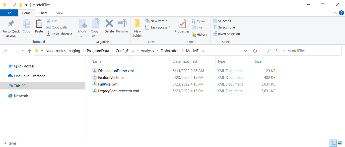
You can leave the other SVM models (.xml) alone. They will not affect anything.
2 - Open Analysis Parameters Dialog
Open the Analysis Parameters dialog for the Dislocation Defect analyzer.
2.1 - Navigate to Analysis Parameters Dialog
In nSpec, navigate to nSpec Main View > Analysis > Edit Parameters…
If the Dislocation Defect analyzer is not pre-selected, select the Dislocation Defect Analyzer in the Analysis combo box at the top of the Analysis Parameters dialog.
2.2 - Select nJson File
NOTE: If you deleted the Default.nJson file (and therefore only have one nJson in the C:\Nanotronics Imaging\ProgramData\ConfigFiles\Analysis\Dislocation directory), you may go to step 2.3.
If you have more than one nJson file in the C:\Nanotronics Imaging\ProgramData\ConfigFiles\Analysis\Dislocation directory, you will get the following dialog:
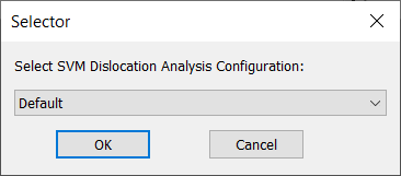
Please select your desired nJson using the combo box and press OK.
2.3 - Understand The Save Button
When you first see the Analysis Parameters dialog, you will notice that the Save button is enabled. Furthermore, if you select another parameter group within the Dislocation Defect analyzer or select another analyzer, you will get a warning that your parameter group has not been saved.
The reason for this that the Dislocation Defect analyzer has two completely hidden parameters that automatically get filled in when you open the Analysis Parameters dialog:
JsonConfigTextJsonConfigFilePath
Just be aware that this functionality happens every single time you entire this dialog.
3 - Set Parameters
At this point, the Dislocation Defect analyzer is just like every other analyzer in terms of setting parameters.
Dislocation Defect Analyzer Parameters
Below is a summary of all the available Dislocation Defect analyzer parameters.
Parameter | Description | Advice |
|---|---|---|
Configuration File Path | Absolute path to model file |
|
configFileName | Name of model file in ModelFiles folder |
|
Calculate Exclusion Info | In the exported CSV report, state whether each defect is in the included wafer area. | |
Look for Non-Chain Dislocation defects | Look for non-chain dislocation defects | |
Export CSV Containing Defect Info | Export a report containing defect data to a CSV. |
|
Look for Chain Defects | Look for chain defects. Turning this option means corner masking will be performed. | |
Minimum Chain Eccentricity | Minimum chain eccentricity | |
Minimum Chain Area | (Micrometers Squared) Minimum chain area. | |
Minimum Dislocation Defect Area | (Micrometers Squared) Minimum chain area. | |
Use Automatic Thresholding. | Use automatic thresholding. | |
Manual Threshold Value | Manual threshold value. Only relevant if automatic thresholding is off. | |
Use Automatic Corner thresholding | Use automatic thresholding when looking for corners. Only relevant if doing corner masking. | |
Manual Corner Threshold | Manual Corner Threshold. Only relevant if automatic corner thresholding is off. | |
Force Corner Masking | Force corner masking regardless of whether or not the analyzer is looking for chains. | |
Minimum Corner Side Length | (Micrometers) Minimum side length of the stage as it appears on images of the wafer's edge. | |
Calculate chain area ratio data | Export data relating the area of chains to the area of component defects. | |
Chain area overlap percentage | The overlap of component defects that create chains. Only used in chain area ratio calculations. | |
Exclude Other defects | Exclude (ignore) defects that classified as Other. | |
Export JSON | Set to TRUE to export analysis results to JSON file. Set to FALSE to disable. |
Export To CSV
All historical versions of the Dislocation Defect analyzer had an option to export to CSV. The output CSV of each of these analyzers had the same column structure but different parameters.
Under C:\Nanotronics Imaging\ProgramData\ConfigFiles\Analysis\Dislocation\Queries, there is a SQL file that is used to prepare the data for the Export CSV Containing Defect Info analysis parameter. This file query execution depends on temporary view that is created just before launching the analysis. Do not touch, modify, remove, rename, or do anything with this file.
New Features
Highlights
NSPEC-4628: Cropped Images Analyzer
For some time nSpec has had a stand-alone utility to filter and crop defects, and within the Device Inspection analyzer. Now, nSpec supports this functionality in the form of a separate and generic post-analysis analyzer. As a post-analysis, this analyzer operates on any previously executed analysis, which means that randomized defect cropping & exporting can now be extended to all results across nSpec.
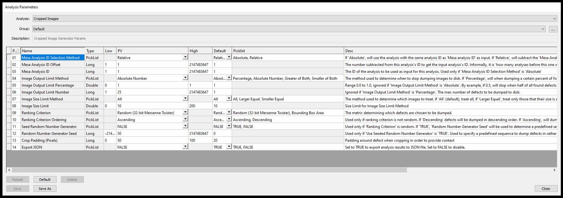
There are a lot of parameters available to customize the cropping behavior. We recommend exploring these options in depth first-hand to best fit for your application.
Unlike the standalone filter and crop feature within nSpec, this analyzer does not require Defect Contours to be exported to the image database to work.
This analysis is best leveraged by saving it to an Analysis Group in tandem with another analysis, as part of an inspection Job. When doing so, make sure that Mesa Analysis ID Selection Method is set to Relative, with the appropriate Mesa Analysis ID Offset targeting the previous analysis with a value of 1. For analysis groups that run more than 2 analyzers, this offset may need to be higher. To add some padding around the cropped defects, use Crop Padding (Pixels), which will allow you to see some context around the defect when reviewing these images outside of nSpec.
For questions and guidance on how to set up , contact support@nanotronics.co.
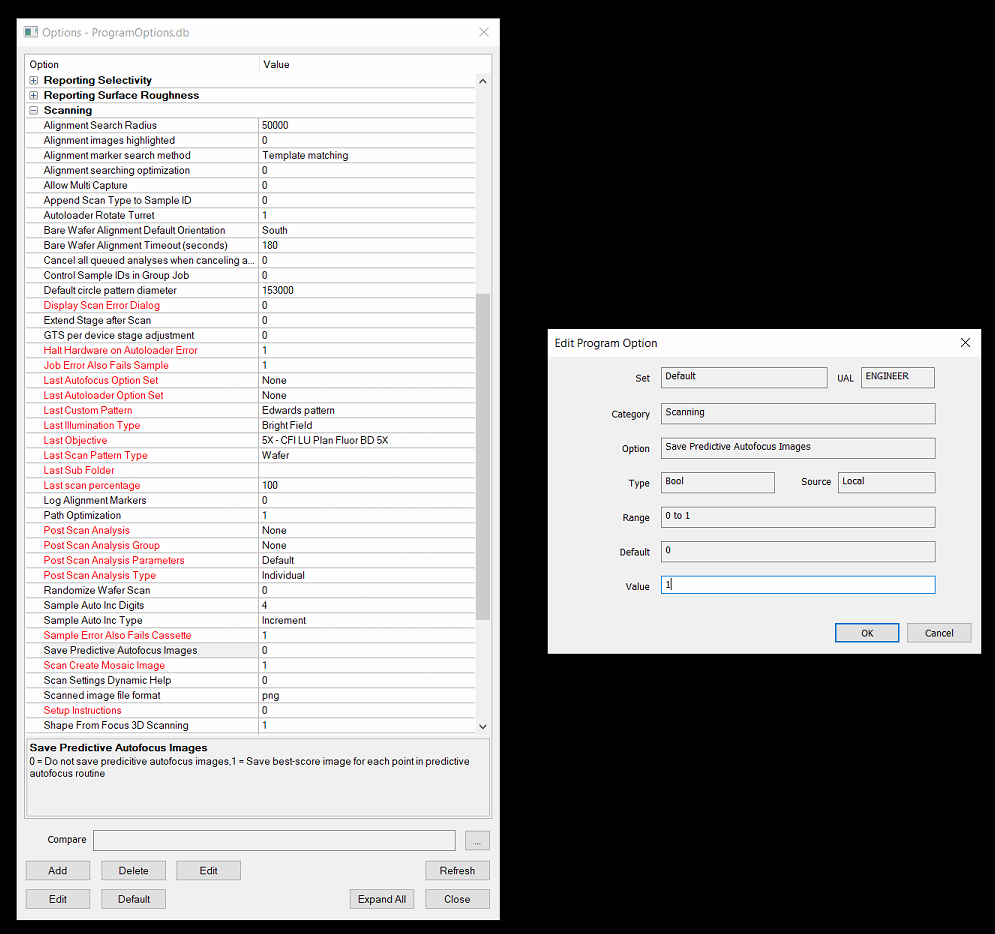
NSPEC-5696: Saved Focus Point Images
One of our goals with this release was to improve users' ability to understand the quality of scanning focus across recipes. This feature allows users to save images representing the final focus capture for each focus point in the predictive focus point pattern alongside a scan. These images can be used as a reference to to help troubleshoot any focus issues that may arise during inspection.
To save images for your focus patterns, open Program Options, and under the Scanning section set Save Predictive Autofocus Images to 1.
After scanning a sample, you should now see a folder alongside your scan images:
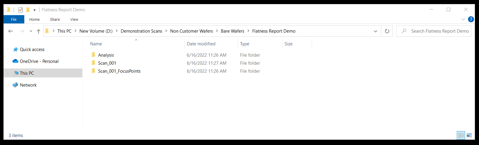
Inside this folder you will see the images captured during autofocus:
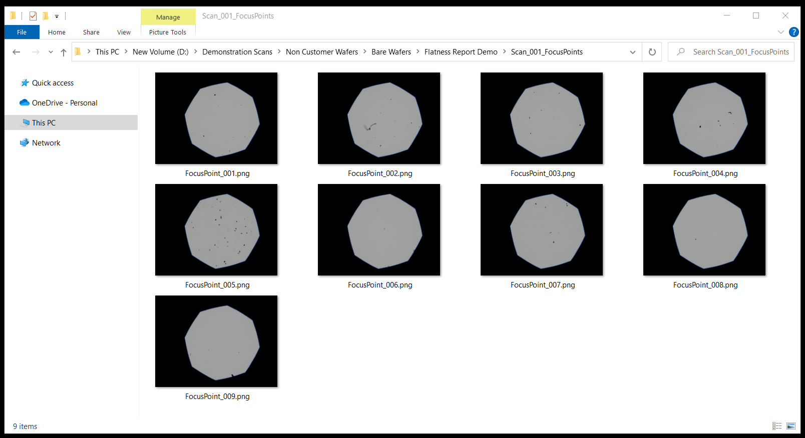
This can be extremely valuable for troubleshooting root cause for any focus quality anomalies during inspection.
NSPEC-5541: Increase Font Size on Device Mark in nView
Over the years we have received a number of requests to improve legibility of device names (IDs, indexes, names, within nView reports, since the font often blends in with high contrast device patterns. In v0.21.1.0 we introduced some visual improvements in nSpec’s Live View to make this easier. In v0.22.0.0 we have extended these improvements to nView as well:
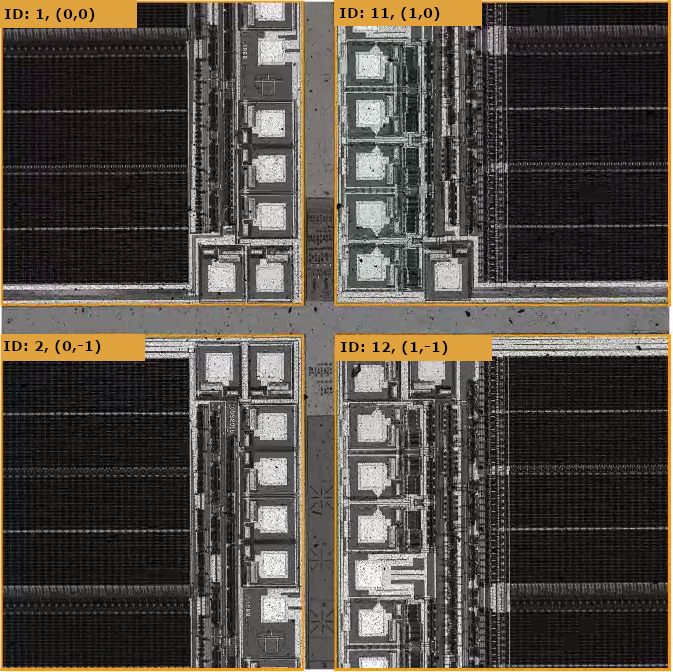
Now, Device naming options are displayed much more legibly. We hope this helps users navigate devices in nView reports with greater ease.
NSPEC-5518: Match Max Zoom Level from Report Image to Live View Image
On the topic of consistency between nSpec Live View and nView reports, we also now support zoom up to 500% within nView reports. This matches the maximum allowable zoom in Live View. This can be helpful when utilizing nView reports for detailed critical dimension review.
NSPEC-5366: Exclude Defects from AI Reports if Outside of Device Boundary
When analyzing a Device Inspection type scan with an AI Analyzer (Gen 3 or Gen 4), there is a new parameter called “Filter Non-Device Defects”. By default this is set to TRUE, which causes the analysis to remove any defects located outside of the device boundary.
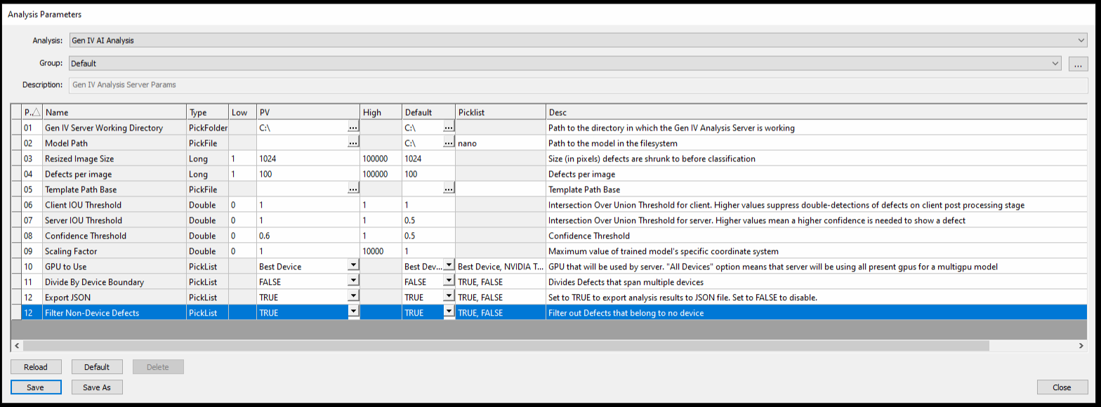
This has the added benefit of removing the possibility of double-counting defects that are visible in more than one image, which can occur with device inspection type scans since image tiles are aligned to the devices, and often include slices of other neighboring devices. To turn off this new default behavior on Gen 3 and Gen 4 AI analyses, simply set this new parameter to FALSE.
Since this new option is TRUE by default, when updating to this version there may be defect count differences before and after the update, if there were previously double-detected defects on AI analyses on device-inspection type scans.
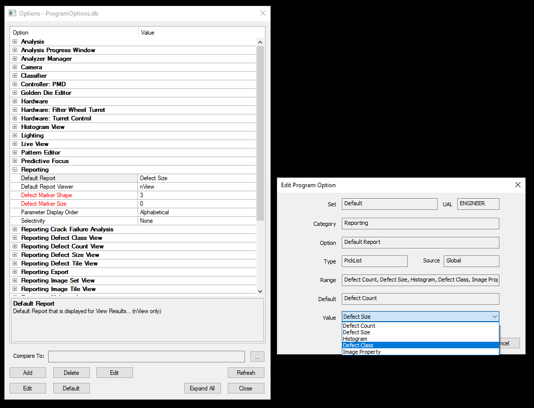
NSPEC-3520: Update Default Report Options
You can now set any report type as the default report to view when opening results in nView. To access these new options, go to Program Options → Reporting → Default Report. Select your primary report type. For AI and Dislocation analyzers, we recommend setting this to Defect Class to get the most out of nSpec Reports.
New Features Changelog
Bug Fixes
Highlights
NSPEC-5789: DI North & South alignment result Offset by various factors
Prior to this fix, some alignment targets were too small to work well with our alignment algorithms, even though the targets were sufficiently unique and visible in the field of view to perform a successful alignment. The behavior in some of these instances was an alignment that snapped to the wrong position, causing devices to scan with a tilt, which sometimes in turn caused analysis stability issues. We have fixed this issue, and fine alignment during device inspection scans should be more robust moving forward.
NSPEC-3907: Fix Edge Exclusion Rendering Issue on Device Inspection Scans
Edge exclusion settings in Program Options no longer applies when viewing defect maps for Device Inspection scans within nView! This bug caused a strange filtering of defects displayed that didn’t reflect any meaningful distribution of defects on the sample. For customers who use both Device Inspection style scans and wafer or pattern type scans with edge exclusion, this will be a major quality of life improvement, since you will no longer need to toggle Edge Exclusion in Program Options every time you switch between the two report types.
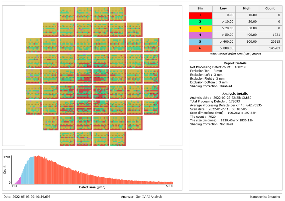
NSPEC-5925: Defect Size Report Histogram is not a Histogram
Histograms now render correctly across all report types in nView! This will help report viewers better understand the distribution of defect area across all defects in the report, which can in turn help users refine analysis parameters to hone in on critical defects.